Optoelectronic element with a non-protruding lens

a technology of optoelectronic elements and lenses, applied in the field of optoelectronics, can solve the problems of low net efficiencies, internal inefficiencies, heat dissipation,

Inactive Publication Date: 2006-06-27
JPMORGAN CHASE BANK NA
View PDF53 Cites 859 Cited by
  • Summary
  • Abstract
  • Description
  • Claims
  • Application Information

AI Technical Summary

Benefits of technology

[0009]An optoelectronic device according to the present invention incorporates a lens that increases component performance. For example, the output of an LED utilizing the lens is increased by, in part, reducing internal reflection. Internal reflection results from the differing indices of refraction at the interface between the LED encapsulant and the surrounding air.
[0011]An optoelectronic device according to the present invention has an encapsulant that functions as a lens. For emitter applications, the lens reduces internal reflection and dispersion without having a protruding curved surface. Thus, LEDs utilizing the present invention have an improved efficiency compared with prior art flatsurfaced LEDs and similar devices, without the physical interface difficulties of the prior art curved-surface LEDs and similar devices. For detector applications, the lens focuses photons on the active area of the detector, increasing detector sensitivity. This increased detector sensitivity allows a detector having a reduced size, hence a reduced cost, to be used for a given application.
[0014]Typically, a look up table or the like correlates the Ratio to saturation. The use of conventional LEDs within pulse oximetry probes has a number of drawbacks. Pulse oximetry performance is limited by signal-to-noise ratio which, in turn, is improved by high light output emitters. LEDs without lenses, such as illustrated in FIG. 1, are not optimized to transmit the maximum amount of light into the skin. LEDs with-protruding lenses, such as illustrated in FIG. 2, create increased pressure on the skin, resulting in perfusion necrosis, i.e. a reduction of arterial blood flow, which is the medium to be measured. A solution to this problem in accordance with the present invention is an LED incorporating a non-protruding lens.
[0016]Another aspect of the present invention is a mold tool for an optoelectronic device that comprises a first mold piece having a surface that defines a first cavity and an aperture within the first cavity. The mold tool also comprises a second mold piece having a surface which defines a second cavity. The first cavity and second cavity cooperate to form a molding compound into a predetermined shape. The mold tool further comprises an ejector pin having a contoured tip. The pin is movably located within the aperture between a first position retracted within the cavity and a second position extended from the aperture. In the first position, the tip constitutes an integral portion of the first cavity. In the second position, the ejector pin facilitates removal of the compound from the first cavity. The ejector pin tip at least partially defines the predetermined shape.
[0018]Yet another aspect of the present invention is an optoelectronic device comprising an encapsulant means for embedding an optoelectronic element and a lens means for conveying light between the optoelectronic element and a media surrounding the encapsulant means. In one embodiment, the optoelectronic device further comprises a flat surface means for providing a low-pressure contact surface for the lens means. In that embodiment, the optoelectronic device can further comprise an arcuate surface means for avoiding total internal reflection of light from the flat surface means. In another embodiment, the optoelectronic device further comprises a surrounding surface means for providing a contact surface for the encapsulant from which the lens means does not protrude.

Problems solved by technology

Internal inefficiencies within a semiconductor diode result in very low net efficiencies, which is the ratio of emitted light power to input power.
Internal inefficiencies arise from a low ratio of minority carriers injected into the diode semiconductor junction to photons generated at the junction; photon loss due to internal reflection at the semiconductor / encapsulant interface; and absorption of photons within the semiconductor material.
Because of these low net efficiencies, many LED applications require high input current, resulting in heat dissipation and device degradation problems in order to obtain sufficient light.
The inefficiencies described above, however, are compounded by the configuration of the LED encapsulant / air interface.
Unfortunately, a protrusion, such as this curved surface, is difficult to accommodate in many applications.

Method used


Image

  • Optoelectronic element with a non-protruding lens
  • Optoelectronic element with a non-protruding lens
  • Optoelectronic element with a non-protruding lens

Examples


Embodiment Construction

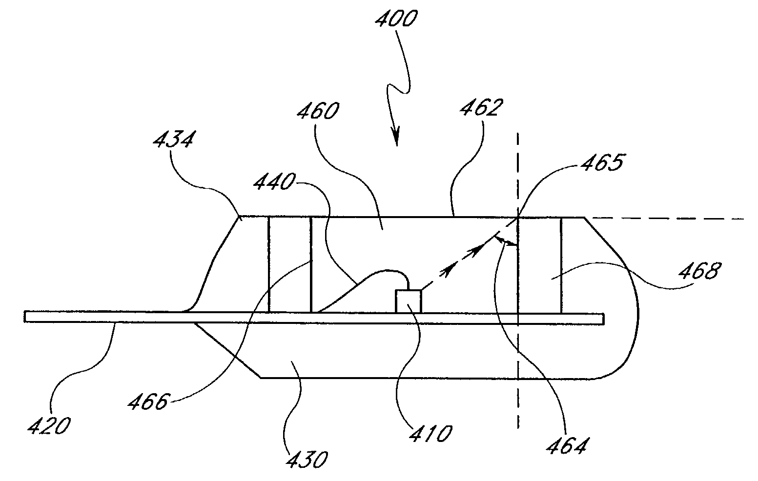
[0036]FIG. 4 illustrates an embodiment of an LED having a non-protruding or minimally protruding lens according to the present invention. The LED 400 consists of at least one semiconductor diode element 410, which is mounted to one lead of a leadframe 420 and connected to another lead of a leadframe 420 with a bond wire 440. The diode element 410, bond wire 440 and portions of the leadframe 420 are surrounded by an encapsulant 430. A lens 460 is molded into a portion of the encapsulant 430. The lens 460 has a generally flat, surface portion 462 that is at or below the plane of the surrounding surface portions 434 of the encapsulant 430. The lens extends radially from the diode element 410 out to the critical angle 464, at which point total internal reflection of photons emitted from the diode element would occur. Past the critical angle 464, the lens 460 has a steep side surface portion 466, which extends below the surface of the surrounding filler portion 434 of the encapsulant 430...


PUM

PropertyMeasurementUnit
critical angleaaaaaaaaaa

Abstract

An optoelectronic component has a lens that is formed in the surface of an encapsulant surrounding a semiconductor diode element. With respect to emitters, the lens reduces internal reflection and reduces dispersion to increase overall efficiency. With respect to detectors, the lens focuses photons on the active area of the detector, increasing detector sensitivity, which allows a detector having a reduced size and reduced cost for a given application. The lens portion of the encapsulant is generally nonprotruding from the surrounding portions of the encapsulant reducing contact surface pressure caused by the optoelectronic component. This non-protruding lens is particularly useful in pulse oximetry sensor applications. The lens is advantageously formed with a contoured-tip ejector pin incorporated into the encapsulant transfer mold, and the lens shape facilitates mold release.

Description

CLAIM OF PRIORITY[0001]This application is a continuation application of, and claims priority from U.S. patent application No. 09 / 038,494, filed Mar. 10, 1998, issued as U.S. Pat. No. 6,525,386, which is incorporated in its entirety by reference herein. This application is also related to U.S. patent application No. 10 / 336,953, filed on Jan. 3, 2003.BACKGROUND OF THE INVENTION[0002]1. Field of the Invention[0003]This invention relates to the field of optoelectronics, which includes light emitting components, such as light emitting diodes (LED) and laser diodes, and which also includes light detecting components, such as photodiodes, phototransistors, photodarlingtons and photovoltaic cells. Optoelectronics also includes various devices which incorporate optoelectronic components, such as displays, photosensors, optocouplers, and fiberoptic transmitters and receivers. In particular, this invention relates to lenses to increase the efficiency of optoelectronic emitters and the sensiti...

Claims


Application Information

Patent Timeline
Patent Type & Authority Patents(United States)
IPC IPC(8): H01L31/0203A61B5/00H01L25/075H01L31/0232H01L33/54
CPCB29C45/401H01L31/0203H01L31/0232H01L33/54A61B5/1455H01L2924/1815H01L24/45H01L25/0753H01L2224/45144H01L2224/48091H01L2924/01077H01L2924/01079B29C45/14655H01L2224/48247Y10S425/808H01L2924/12041H01L2924/00014H01L31/02327H01L2924/12042H01L2924/12043H01L2924/181H01L2924/00H01L2924/00012
Inventor MILLS, MICHAEL A.COFFIN, IV, JAMES P.
Owner JPMORGAN CHASE BANK NA
Why Eureka
Try Eureka