Optical waveguide device, an optical modulator, a mounting structure for an optical waveguide device and a supporting member for an optical waveguide substrate

a technology of optical waveguide and mounting structure, applied in the direction of optical waveguide light guide, optical waveguide, optics, etc., can solve the problem of microwave transmission loss, and achieve the effect of reducing rippl

Inactive Publication Date: 2006-06-27
NGK INSULATORS LTD
View PDF18 Cites 14 Cited by
  • Summary
  • Abstract
  • Description
  • Claims
  • Application Information

AI Technical Summary

Benefits of technology

[0079]It is thus possible to realize the same kind of contact with a CPW probe and to prevent the radiation of unnecessary waves into the supporting body in the direction of thickness, thereby shifting the ripple due to the resonance to a higher frequency range.
[0080]In a preferred embodiment, the conductive layer covers at least a region of the opposing face under the feedthrough portion. FIGS. 11 to 14 relate to this embodiment. FIG. 11 is a plan view schematically showing an optical waveguide device 1G, FIG. 12 is an enlarged view of the feedthrough portion shown in FIG. 11, FIG. 13 is a cross sectional view of the device of FIG. 11 cut along a line XIII—XIII, and FIG. 14 is a cross sectional view of the device of FIG. 11 along a XIV—XIV line.
[0081]Each of the main and supporting bodies 12, 18 has a shape of a plate. Optical waveguides 4A, 4B and 4C of Mach-Zehnder pattern are provided on the main face of the main body 12. A signal electrode 3B is provided between a pair of ground electrodes 3A and 3C.
[0082]A space 19 is formed on a supporting face 18a of a supporting body 18, as can be seen in FIG. 13. Preferably, the space 19 is defined by a smooth and curved face. The shape of the main body 12 is substantially the same as that shown in FIG. 2. A joining layer 6B is interposed between the opposing face 18a of the body 18 and a base portion 12e the main body 12, for joining the bodies 12 and 18. 20D is a supporting member.
[0083]In the example shown in FIG. 11, a pair of feedthrough portions 32A and 32B are provided for the electrodes 3A, 3B and 3C. In each feedthrough portion, the signal electrode 3B has an end part 30 with a larger width. The electrode gaps 5a and 5b between the signal electrode 3B and ground electrodes 3A, 3C are widened in the end portion 30. The widened end portion 30 and gaps are provided in each feedthrough portion for the matching of characteristic impedance with an outer electrode provided in an outer connector.
[0084]In the present example, a feedthrough gap 33 is provided between the end part 30a of the signal electrode 30 and the side face 12f of the main body 12, and between the electrode gap 5a or 5b and the side face 12f. Conductive layers 31A and 31B cover regions R2 of the opposing face 18a under the feedthrough gaps 33, respectively. It is thereby possible to reduce the ripple due to substrate radiation from the connecting part of the signal and ground electrodes and an outer connector. R1 is a region of the opposing face 18a under the feedthrough portion 32A or 32B.

Problems solved by technology

The microwave may thereby induce the resonance of the reinforcing supporting body, resulting in a transmission loss of the microwave.

Method used


Image

  • Optical waveguide device, an optical modulator, a mounting structure for an optical waveguide device and a supporting member for an optical waveguide substrate
  • Optical waveguide device, an optical modulator, a mounting structure for an optical waveguide device and a supporting member for an optical waveguide substrate
  • Optical waveguide device, an optical modulator, a mounting structure for an optical waveguide device and a supporting member for an optical waveguide substrate

Examples


example 1

[0092](Example 1)

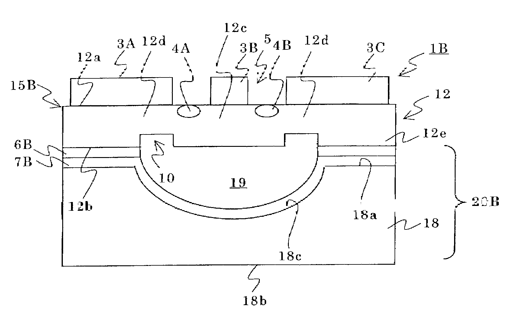
[0093]An optical modulator 1A shown in FIG. 1 was produced. In detail, an X-cut 3 inch wafer (made of LiNbO3 single crystal) was used as a substrate. Optical waveguides 4A, 4B of Mach-Zehnder type were formed in the surface area of the wafer by titanium diffusion and photolithography. The size of the optical waveguide may be set at, for example, 10 μm at 1 / e2. CPW electrodes 3A, 3B and 3C were formed by electroplating. The electrode gaps of the central signal electrode 3B and ground electrodes 3A, 3C were 40 μm, the thickness of each electrode was 30 μm, and the length of the electrode was 40 μm.

[0094]A dummy wafer for grinding was then fixed on a grinding surface plate, and the main body (wafer) for a modulator was adhered onto the dummy wafer with the main face (with the electrodes) facing the dummy wafer. The main body (wafer) 2 for a modulator was then subjected to horizontal grinding, lapping and polishing (CMP) so as to machine the main body 2 to a thickness o...

example 2

[0097](Example 2)

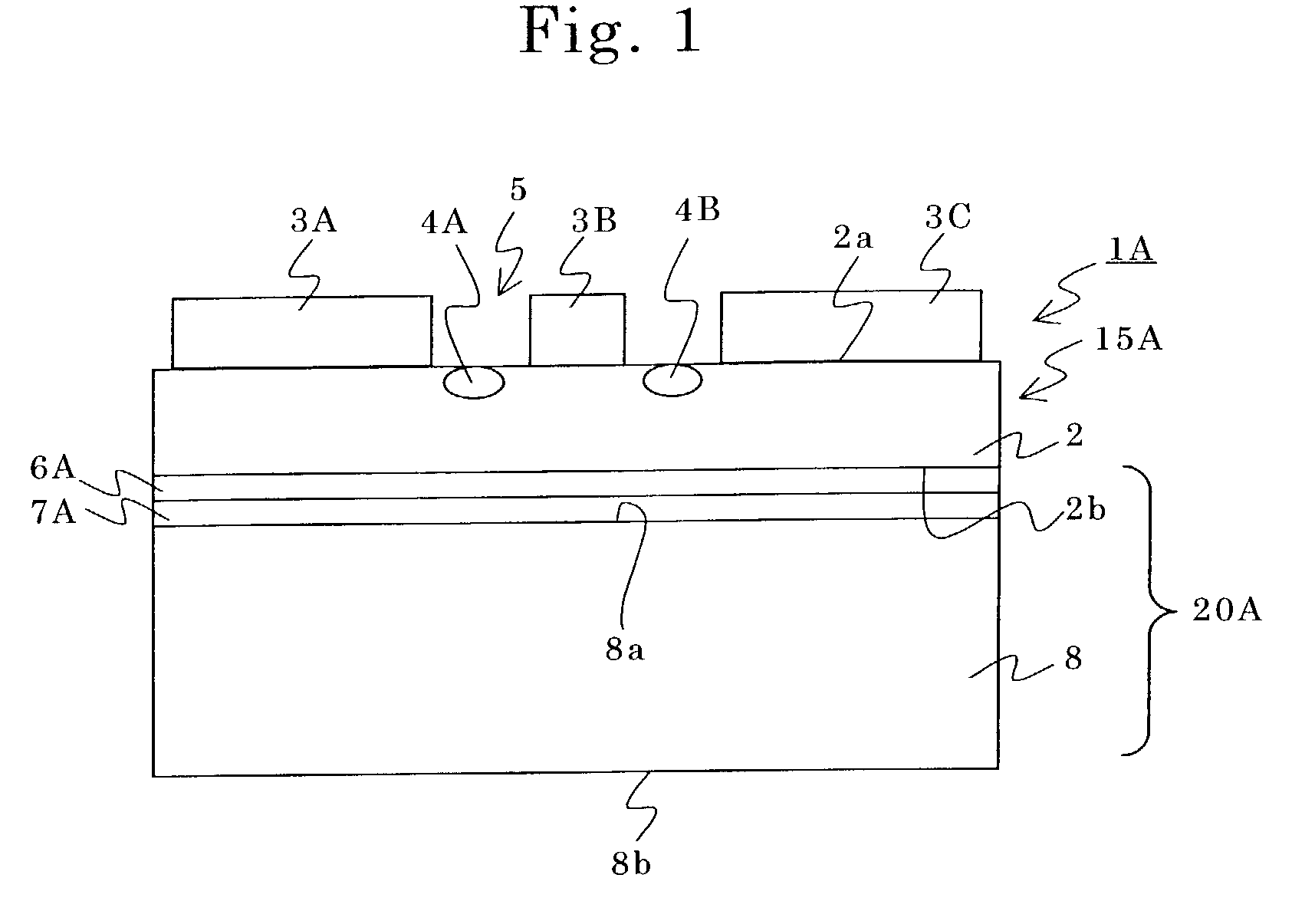
[0098]An optical modulator 1B shown in FIG. 2 was produced. Ti diffusion optical waveguides and CPW electrodes were formed on an X-cut wafer of lithium niobate, as described in the example 1. The shapes and dimensions of the electrodes were the same as those in the example 1. A dummy wafer for grinding was then fixed on a grinding surface plate, and a main body (wafer) for a modulator was adhered onto the dummy wafer with the main face with the electrodes facing the dummy wafer. The main body (wafer) 2 for a modulator was then subjected to horizontal grinding, lapping and polishing (CMP) so as to machine the main body 2 to a thickness of 15 μm. The main body was then worked with an excimer laser at a region near the ground electrodes to a thickness of 10 μm to form a recess 10.

[0099]A space 19 with a width of 0.3 mm and a depth of 0.1 mm was formed in a supporting body 18. A conductive layer 7B of Au with a thickness of 1 μm was then formed on the opposing faces 18a...

example 3

[0102](Example 3)

[0103]An optical modulator 1C shown in FIG. 3 was produced. The optical waveguide substrate 15C was produced according to the same process as described in the example 2. A conductive layer 7A made of gold with a thickness of 1 μm was formed on the surface of a plate-shaped supporting body 8. A main body for an optical modulator was adhered and fixed onto the supporting body 8, using a film-shaped epoxy resin with a thickness of 100 μm, to produce a wafer having optical modulators 1C. The resulting wafer was then cut with a dicing machine to obtain chips. Each chip 1C had a width of 4.4 μm and a total thickness of 1 mm.

[0104]The S21 property measured was the same as example 1. A ripple was not observed within a frequency range measured.


PUM

PropertyMeasurementUnit
thicknessaaaaaaaaaa
thicknessaaaaaaaaaa
frequencyaaaaaaaaaa

Abstract

An optical waveguide device has an optical waveguide substrate and a supporting body for supporting the substrate. The substrate has a main body made of an electro-optic material and having a main face and an opposing face, optical waveguides, and electrodes for applying an electrical signal on the optical waveguides. At least a part of the opposing face of the supporting body opposing the substrate is covered with a conductive layer. It is thus possible to reduce the resonance due to substrate radiation leakage of the microwave signal into the whole of the optical waveguide substrate and supporting body.

Description

[0001]This application claims the benefit of Japanese Patent Applications P2001-268680, filed on Sep. 5, 2001, and P2002-219090, filed on Jul. 29, 2002, the entireties of which are incorporated herein by reference.BACKGROUND OF THE INVENTION[0002]1. Field of the Invention[0003]The present invention relates to an optical waveguide device, an optical modulator, a mounting structure for an optical waveguide device and a supporting member for an optical waveguide substrate.[0004]2. Related Art Statement[0005]Recent development of multimedia systems demands a broadband communication network system. An optical transmission system operating on a frequency higher than 10 Gb / s has been already commercialized. Such a system capable of operating on a higher frequency is expected. For example, a lithium niobate optical modulator or a semiconductor filed absorption modulator (Electro-absorption modulator: EA modulator) is used as a device for modulating an electrical signal (microwave signal) wi...

Claims


Application Information

Patent Timeline
Patent Type & Authority Patents(United States)
IPC IPC(8): G02F1/35G02B6/10G02F1/295G02B6/12G02F1/03G02F1/035G02F1/225
CPCG02F1/0356G02F1/2255G02F2201/505
Inventor KONDO, JUNGOKONDO, ATSUOAOKI, KENJIMITOMI, OSAMU
Owner NGK INSULATORS LTD
Why Eureka
Try Eureka