Parallel data interface and method for high-speed timing adjustment

a data interface and parallel data technology, applied in the field of data interfaces, can solve the problems of significantly affecting system performance and/or reliability, the amount of time is comparable to the propagation delay, and the high-speed synchronous system cannot afford significant skewing of the clock signal, so as to reduce the overall power consumed by the data interface and provide flexibility to users

Inactive Publication Date: 2006-06-27
RPX CORP
View PDF5 Cites 92 Cited by
  • Summary
  • Abstract
  • Description
  • Claims
  • Application Information

AI Technical Summary

Benefits of technology

[0017]The problems outlined above may be in large part addressed by a parallel data interface that adjusts a timing relationship of a clock signal to not only minimize clock skew, but to also compensate for noise components, such as data skew and jitter, which may affect one or more paths of a parallel data bus. In this manner, a plurality of data signals having dissimilar transition times can be accurately sampled by adjusting a clock transition to occur at a time that best suits substantially all of the plurality of data signals. As such, the data interface provides error-free data transmission regardless of unpredictable timing delays along the clock and / or data paths. In general, such a data interface may be included within transmitting and / or receiving portions of any synchronous system.
[0018]In some embodiments, the parallel data interface preferably includes a first phase generator coupled to generate a first plurality of time delay pulses. In addition, the parallel data interface preferably includes a first phase selector coupled to select one of the first plurality of time delay pulses (i.e., a “best phase”) to adjust the timing of a clock signal to accurately sample each and every one of the plurality of data signals of the parallel data bus. In other words, the parallel data interface is adapted to temporally shift a transition of the clock signal by the select one of the first plurality of time delay pulses to sample each and every one of the plurality of data signals without the occurrence of a bit error.
[0020]Moreover, the parallel data interface preferably includes a test access port coupled to the control signal generator. In some cases, the test access port may be a serial port including at least one input pin of the data interface. In other cases, however, the test access port may be a parallel port including a plurality of input pins of the data interface. In any case, the test access port generally includes a number of input pins substantially less than the number of phases generated by the phase generator. In addition, calibration signals input to the test access port may enable the control signal generator to begin a calibration process, or alternatively, to provide previously calibrated control signals to the phase generator. In the latter case, previously calibrated control signals result from hardwiring a “best phase” control signal after performing a previous calibration process to characterize a timing relationship between signals traversing a clock path and each and every one of the paths of the parallel data bus. Preferably, the hardwired control signal is implemented with re-programmable circuit elements, which advantageously reduces the overall power consumed by the data interface while providing the user with flexibility in tailoring the data interface to one or more specific applications.

Problems solved by technology

In some cases, the amount of time is comparable to the propagation delay through output latches of the data interface within the receiving portion.
As such, high-speed synchronous systems usually cannot afford significant skewing of the clock signal relative to data signal transitions.
Because clock signals are used to drive many of the components within synchronous systems, any variation in the arrival of a clock transition may significantly impact system performance and / or reliability.
In some cases, clock skew significantly affects the timing margins of synchronous systems, such as setup, hold, and access time margins, by decreasing the predictability of the arrival of a clock transition.
In some cases, however, clock skew may shift the clock transition sufficiently in time to cause a bit error to occur when the data is sampled.
A bit error, as described herein, is a sampling error that occurs when a clock transition incorrectly samples a data signal.
In addition, clock skew may reduce the cycle time within which information can be passed from one device to the next.
As system speeds increase, clock skew may become an increasingly large portion of the total cycle time.
If clock skew exceeds such an allocated amount, the system will most likely perform unreliably.
Although numerous techniques are used in an effort to minimize clock skew, most techniques cannot in all conditions ensure a data signal transition occurs at the critical moment between clock signal edges.
The selection of delay amounts, however, is undesirably fixed by the circuit design and cannot be changed by the user.
A PLD, however, generally exhibits low operating speeds, such as operating speeds of 150 MHz or below.
As such, a PLD may not be fast enough to accommodate high-speed synchronous systems having operating speeds substantially greater than 150 MHz.
An application specific integrated circuit (ASIC), on the other hand, may provide a variable amount of delay to the clock path at possibly higher operating speeds than a PLD.
ASICs, however, are typically very expensive and their performance is often highly sensitive to any impedance mismatches at the inputs and outputs of the device.
In addition, adding any external component tends to undesirably increase the financial cost, power, and area consumed by the synchronous system.
One disadvantage of internal data interface 10, however, is that the amount of delay imparted to the clock path is undesirably fixed by the circuit design.
In addition, though internal data interface 10 provides a substantially consistent amount of clock path delay, it does not guarantee that the timing along the data path is correct.
In a synchronous system, for example, which utilizes a parallel data bus (i.e., a plurality of parallel data paths) to transfer data between transmitting and receiving portions, interference between individual paths of the parallel data bus may introduce an unpredictable amount of delay to one or more of the individual paths.
As such, even though internal data interface 10 may reduce the affects of clock skew, interference within the parallel data bus may skew the data signals separate from one another thereby causing one or more of the data signals to be sampled incorrectly.

Method used


Image

  • Parallel data interface and method for high-speed timing adjustment
  • Parallel data interface and method for high-speed timing adjustment
  • Parallel data interface and method for high-speed timing adjustment

Examples


Embodiment Construction

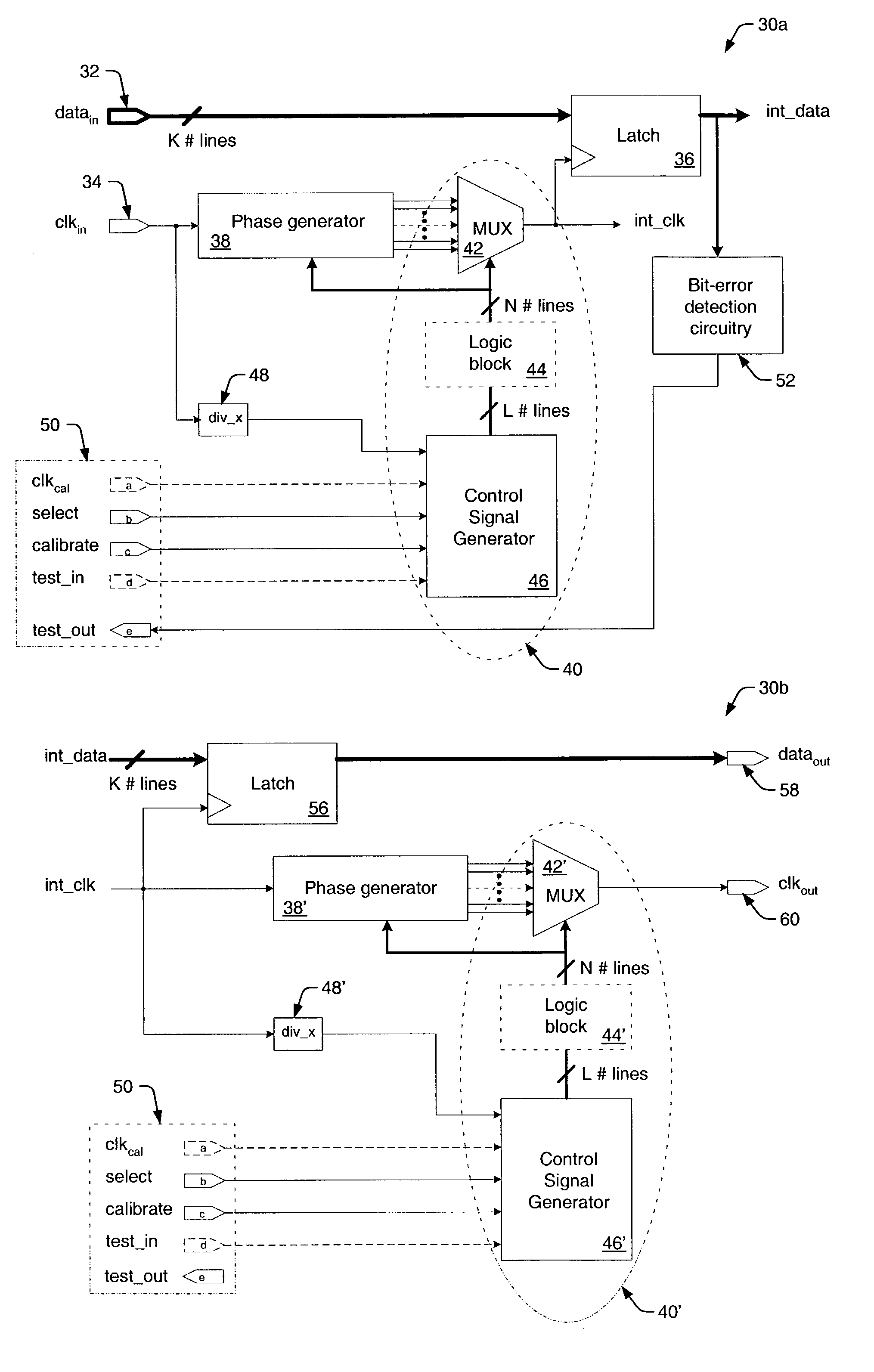
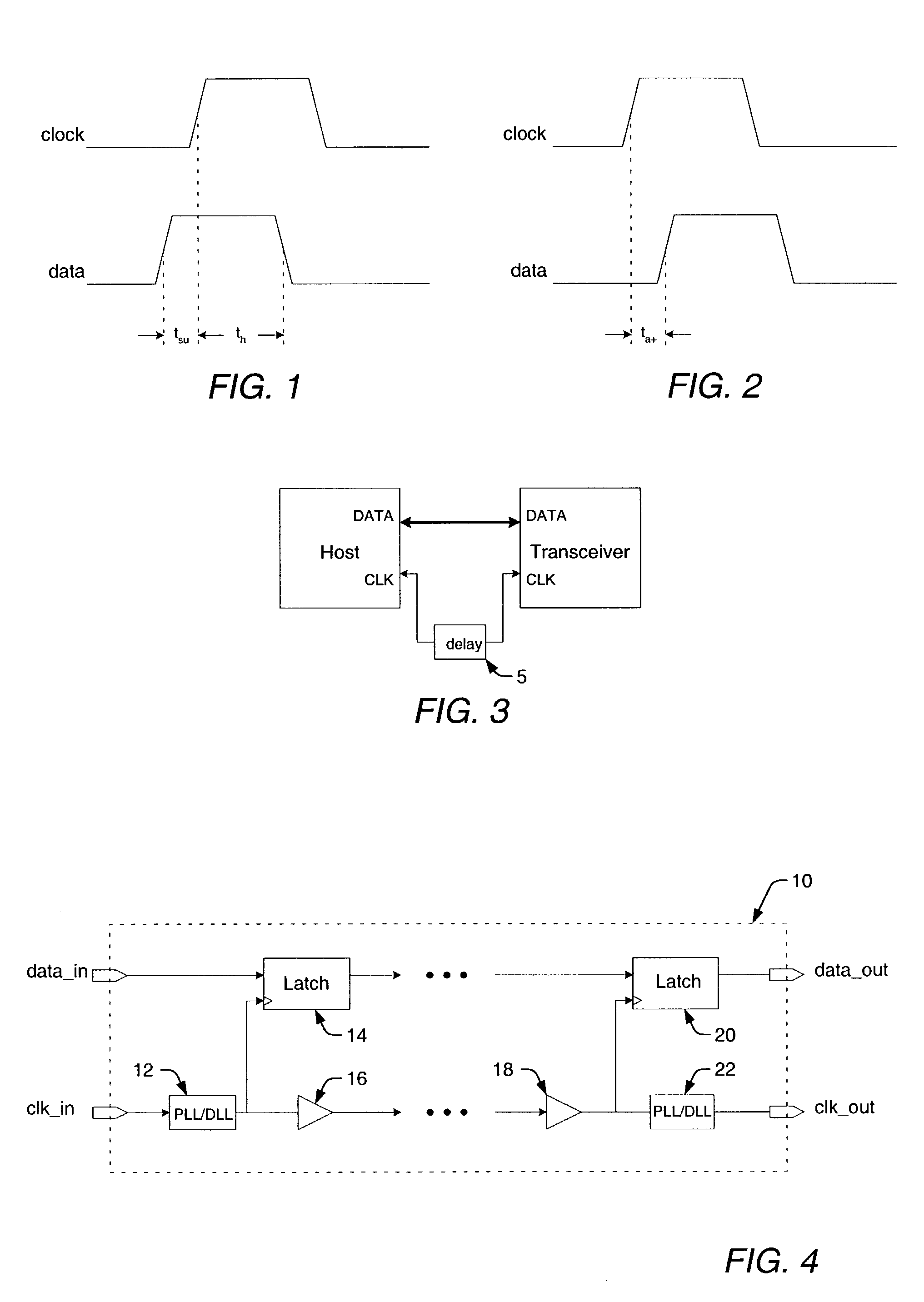
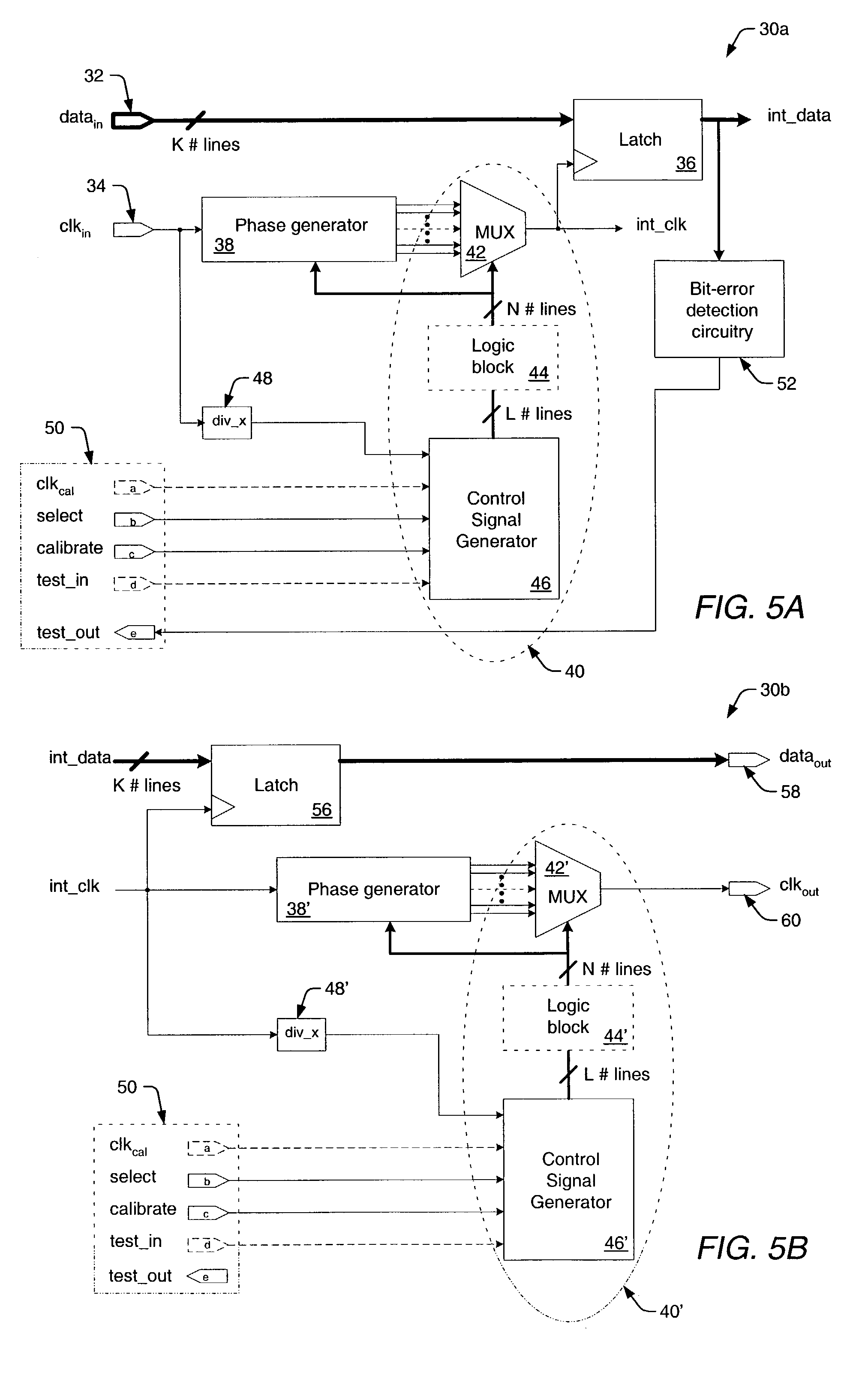
[0045]Error-free data transmission is typically a major design goal for any synchronous system. In high-speed synchronous systems that transmit data over a parallel bus, however, several factors may interfere with obtaining such a design goal. In addition to clock skew, random noise induced within the parallel data bus may adversely effect data transmission. For example, bit errors may result if a sufficient amount of noise is induced within the data bus when the data signal is sampled. In general, noise may be induced in the form of data skew and / or jitter within one or more paths of the parallel data bus. Although they are often caused by similar sources, distinct differences exist between data skew and jitter.

[0046]Data skew is often defined by variations between one data path and another. For example, individual paths of a parallel data bus are generally routed within close proximity to each other. As such, signals traversing a given data path may be adversely affected by noise,...


PUM


Abstract

A parallel data interface and method is provided herein, which adjusts a timing relationship of a clock signal to not only minimize clock skew, but to also compensate for noise components that may affect one or more paths of a parallel data bus. In some embodiments, the parallel data interface includes a first phase generator coupled to generate a first plurality of time delay pulses, and a first phase selector adapted to select one of the first plurality of time delay pulses to adjust the timing of a clock signal to sample each and every one of the plurality of data signals between minimum setup and hold time thresholds. In some embodiments, the parallel data interface includes a second phase generator coupled to generate a second plurality of time delay pulses, and a second phase selector adapted to select one of the second plurality of time delay pulses to adjust the timing of the clock signal to output the plurality of data signals from the data interface at least an amount of time (i.e., an access time) after the adjusted clock transition is output from the data interface.

Description

BACKGROUND OF THE INVENTION[0001]1. Field of the Invention[0002]This invention relates to a data interface that receives a plurality of data signals from a parallel bus, and accurately samples each and every one of the data signals having dissimilar transition times between transitions of a clock signal. As such, the data interface is adapted to adjust a timing relationship between a clock signal and the plurality of data signals with a relative amount of phase delay imparted to the clock signal. The data interface may be included within a synchronous device or, more particularly, within a communications system or network to receive and / or transmit the plurality of data signals over a parallel data bus.[0003]2. Description of the Related Art[0004]The following descriptions and examples are given as background only.[0005]A synchronous device is a device in which data may be transferred from one edge-sensitive element to another in response to an active transition of a clock signal. S...

Claims


Application Information

Patent Timeline
Patent Type & Authority Patents(United States)
IPC IPC(8): G06F13/42
CPCH04L7/0338H03L7/0996
Inventor SARDI, MOHAMEDLI, GABRIEL M.
Owner RPX CORP
Why Eureka
Try Eureka