Method of fabricating capacitor

a capacitor and dielectric layer technology, applied in the direction of capacitors, semiconductor devices, electrical equipment, etc., can solve the problems of reducing the integration degree of devices, reducing the economic effect of manufacture, and insufficient capacitance per unit area of mis capacitors suitable for high-voltage applications, so as to improve the quality of the capacitor dielectric layer.

Active Publication Date: 2006-07-04
UNITED MICROELECTRONICS CORP
View PDF1 Cites 4 Cited by
  • Summary
  • Abstract
  • Description
  • Claims
  • Application Information

AI Technical Summary

Benefits of technology

[0007]Accordingly, one object of this invention is to provide a method of fabricating a capacitor that can improve the quality of the capacitor dielectric layer.
[0008]Another object of this invention is to provide a method of fabricating a capacitor that can lower the resistance of the capacitor to increase the Q-factor of the same.
[0012]Since the dielectric layer is formed before the doping step, the quality of the dielectric layer under the upper electrode is better. Moreover, by incorporating a salicide process after the lower electrode is formed, the resistance of each of the upper and lower electrodes can be reduced to increase the Q-factor of the capacitor.

Problems solved by technology

However, a MIM or MIS capacitor suitable to high-voltage applications is usually insufficient in the capacitance per unit area.
However, after the semiconductor industry advanced to deep sub-micron generation, increasing the capacitor area will reduce the integration degree of devices more significantly so that the economic effect of manufacture is lowered more.
Nevertheless, since the dielectric layer is formed after the doping step for forming the lower electrode, the quality thereof is not good.
Meanwhile, the dopant concentration in the doped region is not so uniform.
Moreover, the lower electrode constituted of a doped region has a higher resistance than metal, so that the Q-factor of the capacitor is usually too small to satisfy high-frequency applications.

Method used


Image

  • Method of fabricating capacitor
  • Method of fabricating capacitor
  • Method of fabricating capacitor

Examples


first embodiment

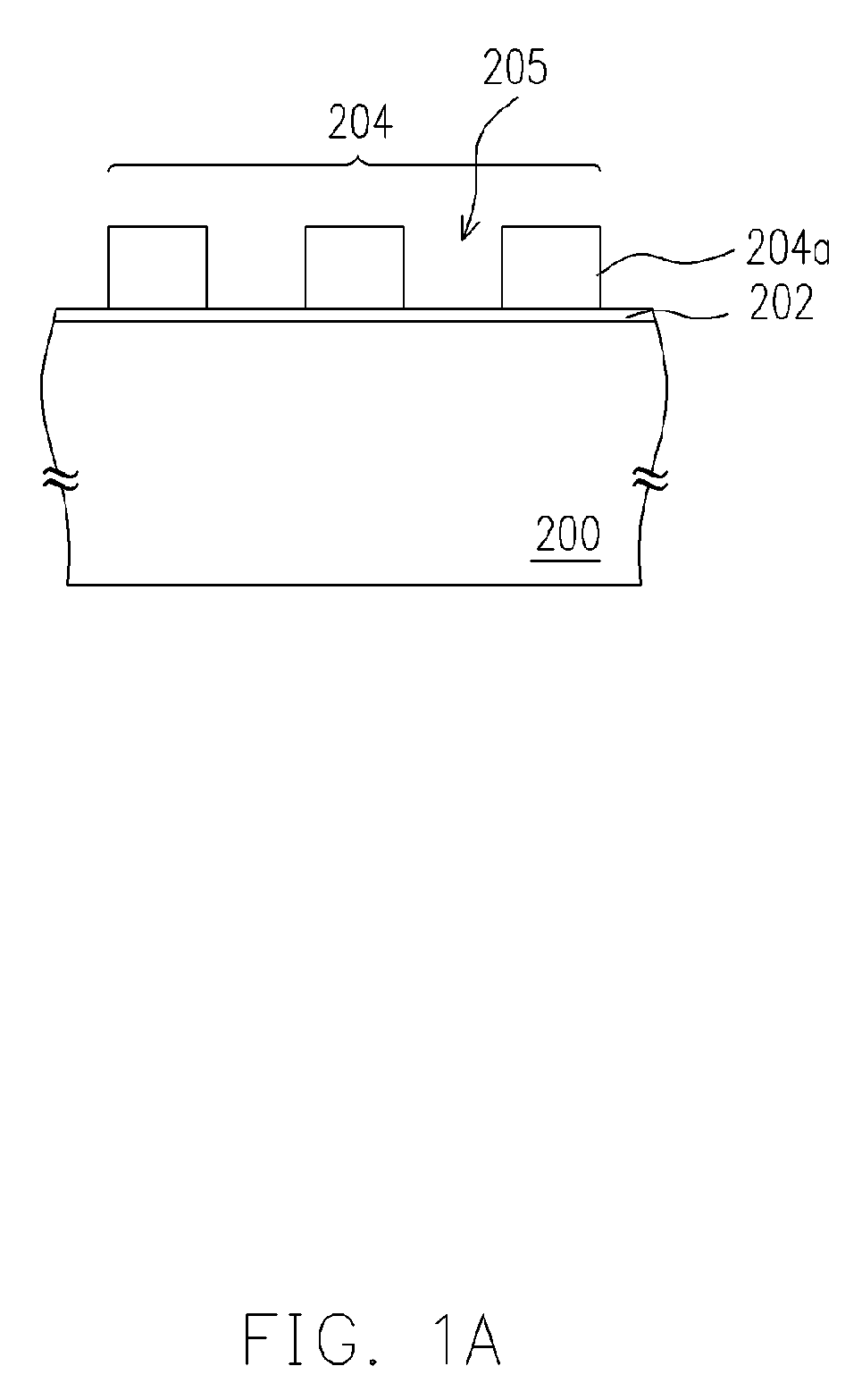
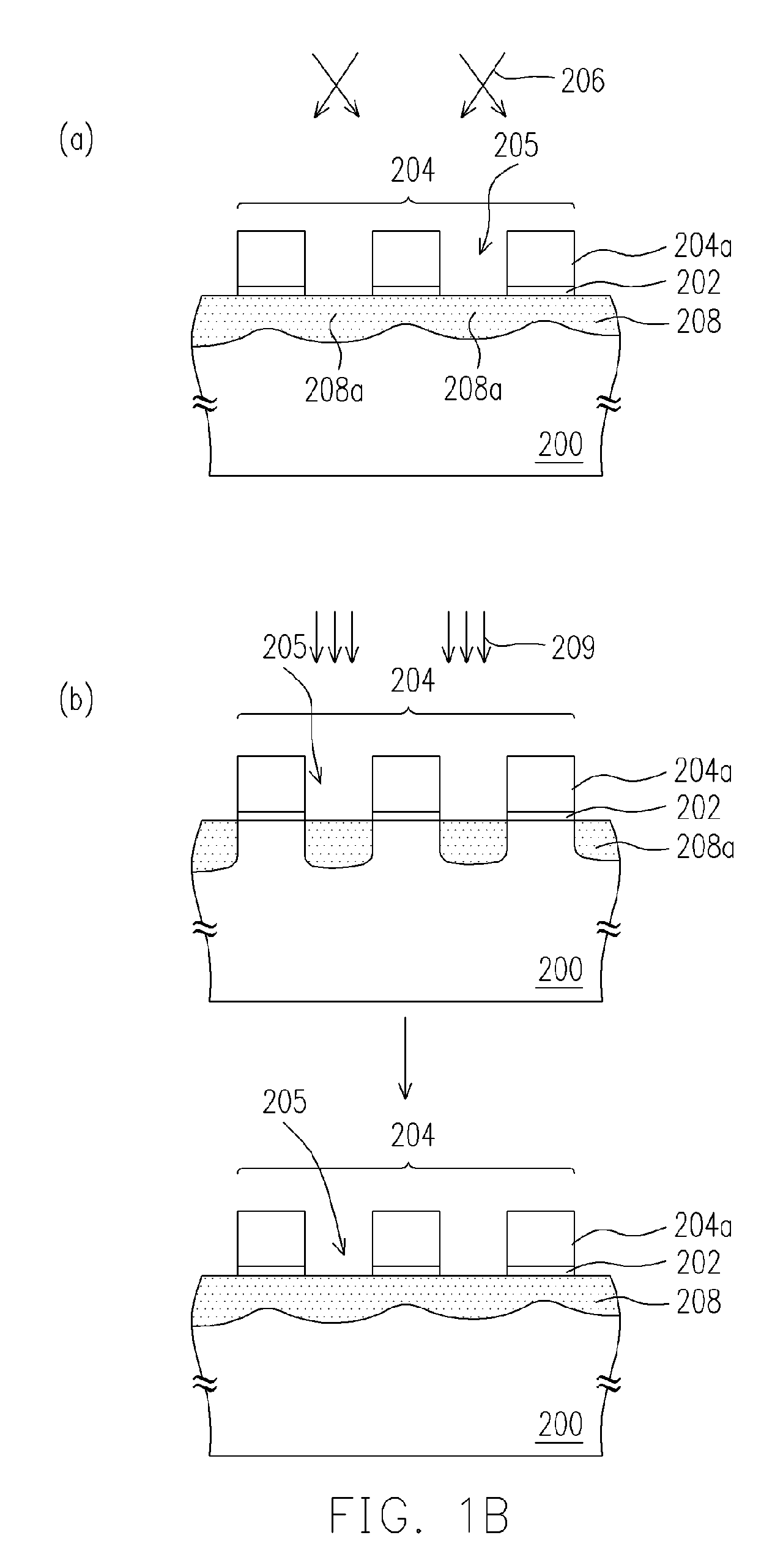
[0020]FIGS. 1A and 1B(a) / (b) illustrate a process flow of fabricating a capacitor according to the first embodiment of this invention in a cross-sectional view, wherein two different doping methods for forming the lower electrode are shown in FIG. 1B(a) and FIG. 1B(b), respectively.

[0021]Referring to FIG. 1A, a semiconductor substrate 200 is provided, which may be a single-crystal silicon substrate. A dielectric layer 202 is formed on the substrate 200, preferably together with the gate dielectric layers in the MOS area (not shown) of the same substrate 200. For example, the dielectric layer 202 can be a silicon oxide layer that is formed simultaneously with the gate oxide layers in the MOS area through thermal oxidation.

[0022]Then, an upper electrode 204 having multiple openings 205 therein is formed on the dielectric layer 202. The steps for forming the upper electrode 204 may include forming a doped polysilicon layer on the dielectric layer 202 and patterning the same with a lith...

second embodiment

[0027]FIGS. 2A–2B illustrate a latter part of a process flow of fabricating a capacitor according to the second embodiment of this invention in a cross-sectional view. The former part of the process flow is described in the first embodiment, while the step of FIG. 2A is subsequent to the step of FIG. 1B and the same elements are labeled with the same reference numbers.

[0028]Referring to FIG. 2A, a spacer 210 is formed on the sidewall of each opening 205 in the upper electrode 204. The spacers 210 may be formed simultaneously with the spacers on the sidewalls of the gates in a MOS area (not shown) on the same substrate 200. The spacers 210 are formed by, for example, forming a conformal insulating layer (not shown) over the substrate 200 and then anisotropically etching the same to remove portions thereof. The material of the insulating layer may be silicon nitride, and the method for forming the same is chemical vapor deposition (CVD), for example.

[0029]Referring to FIG. 2B, a self-...

third embodiment

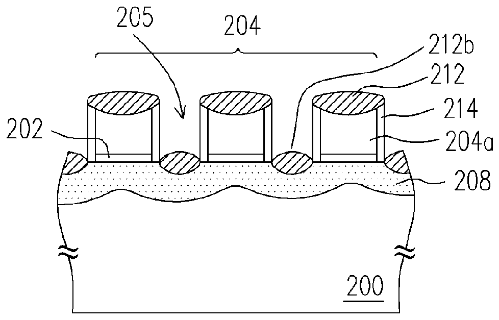
[0031]FIGS. 3A–3B illustrate a latter part of a process flow of fabricating a capacitor according to the third embodiment of this invention in a cross-sectional view. The former part of the process flow is described in the first embodiment, while the step of FIG. 3A is subsequent to the step of FIG. 1B and the same elements are labeled with the same reference numbers.

[0032]Referring to FIG. 3A, after the lower electrode 208 is formed, a liner layer 214 is formed on the sidewall of each opening 205 in the upper electrode 204, and then a spacer 210 is formed on each liner layer 214. The liner layer 214 may include silicon oxide and may be formed with thermal oxidation, for example. The forming method and the material of the spacer 210 may be the same as those in the second embodiment.

[0033]Referring to FIG. 3B, the spacers 210 are removed with, for example, isotropic etching, leaving the liner layers 214 on the sidewalls of the openings 205. It is particularly noted that the liner lay...


PUM

PropertyMeasurementUnit
conductiveaaaaaaaaaa
refractoryaaaaaaaaaa
electrical resistanceaaaaaaaaaa

Abstract

A method of fabricating a capacitor is described. A dielectric layer is formed over a substrate. An upper electrode having multiple openings therein is formed over the dielectric layer. Then, a doping step is performed to the substrate through the openings to form a single doped region as a lower electrode in the substrate under the upper electrode.

Description

BACKGROUND OF THE INVENTION[0001]1. Field of the Invention[0002]The present invention relates to a method of fabricating a semiconductor device. More particularly, the present invention relates to a method of fabricating a capacitor that can improve the quality of the inter-electrode dielectric layer and reduce the electrical resistance of the lower electrode to increase the Q-factor of the capacitor.[0003]2. Description of the Related Art[0004]In the prior art, a capacitor compatible to MOS process usually has a metal-insulator-metal (MIM) structure or metal-insulator-silicon (MIS) structure. However, a MIM or MIS capacitor suitable to high-voltage applications is usually insufficient in the capacitance per unit area. Meanwhile, for mixed-mode devices or RF devices including capacitors, it is frequently required to save a large area of the die for the capacitors to achieve sufficient capacitance satisfying the design rule. However, after the semiconductor industry advanced to deep ...

Claims


Application Information

Patent Timeline
Patent Type & Authority Patents(United States)
IPC IPC(8): H01L21/20
CPCH01L21/26586H01L29/665H01L28/86H01L27/0805
Inventor GAU, JING-HORNG
Owner UNITED MICROELECTRONICS CORP
Why Eureka
Try Eureka