Gated vertical punch through device used as a high performance charge detection amplifier

Active Publication Date: 2006-07-11
ISETEX
View PDF9 Cites 39 Cited by
  • Summary
  • Abstract
  • Description
  • Claims
  • Application Information

AI Technical Summary

Benefits of technology

[0010]The invention provides a practical non-destructive charge detection readout system whose charge conversion factor is high, whose noise floor is reduced by using a sufficiently high channel current in the sensing transistor, and provides a practical high performance charge detection node whose charge handling capacity is hi

Problems solved by technology

The destructive charge readout nodes typically reset charge to a predetermined reference level, which causes generation of kTC noise. kTC noise may be removed from the signal later by a complicated CDS signal processing method.
However, the BCD charge detection system has also some disadvantages.
The main problem is the low conversion gain described by the formula Gc=q/(2*Cg).
The factor 2 appearing in the denominator significantly reduces the conversion gain and makes it less competitive with more conventional structures.
The second significant problem is the current carrying capacity of the overlying MOS transistor.
The current is limited by a compl

Method used


Image

  • Gated vertical punch through device used as a high performance charge detection amplifier
  • Gated vertical punch through device used as a high performance charge detection amplifier
  • Gated vertical punch through device used as a high performance charge detection amplifier

Examples


Embodiment Construction

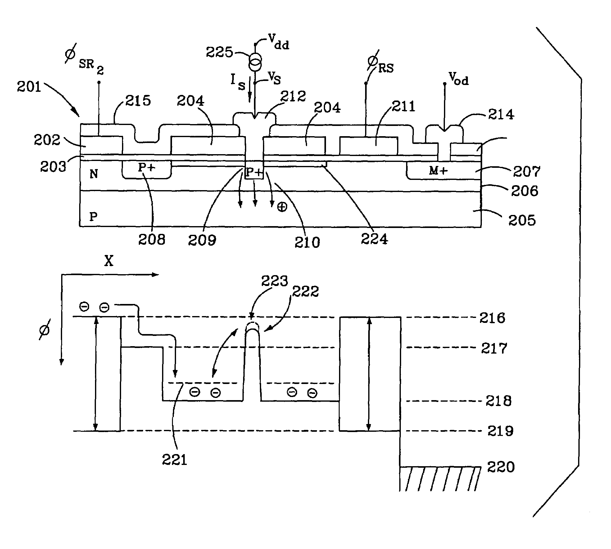
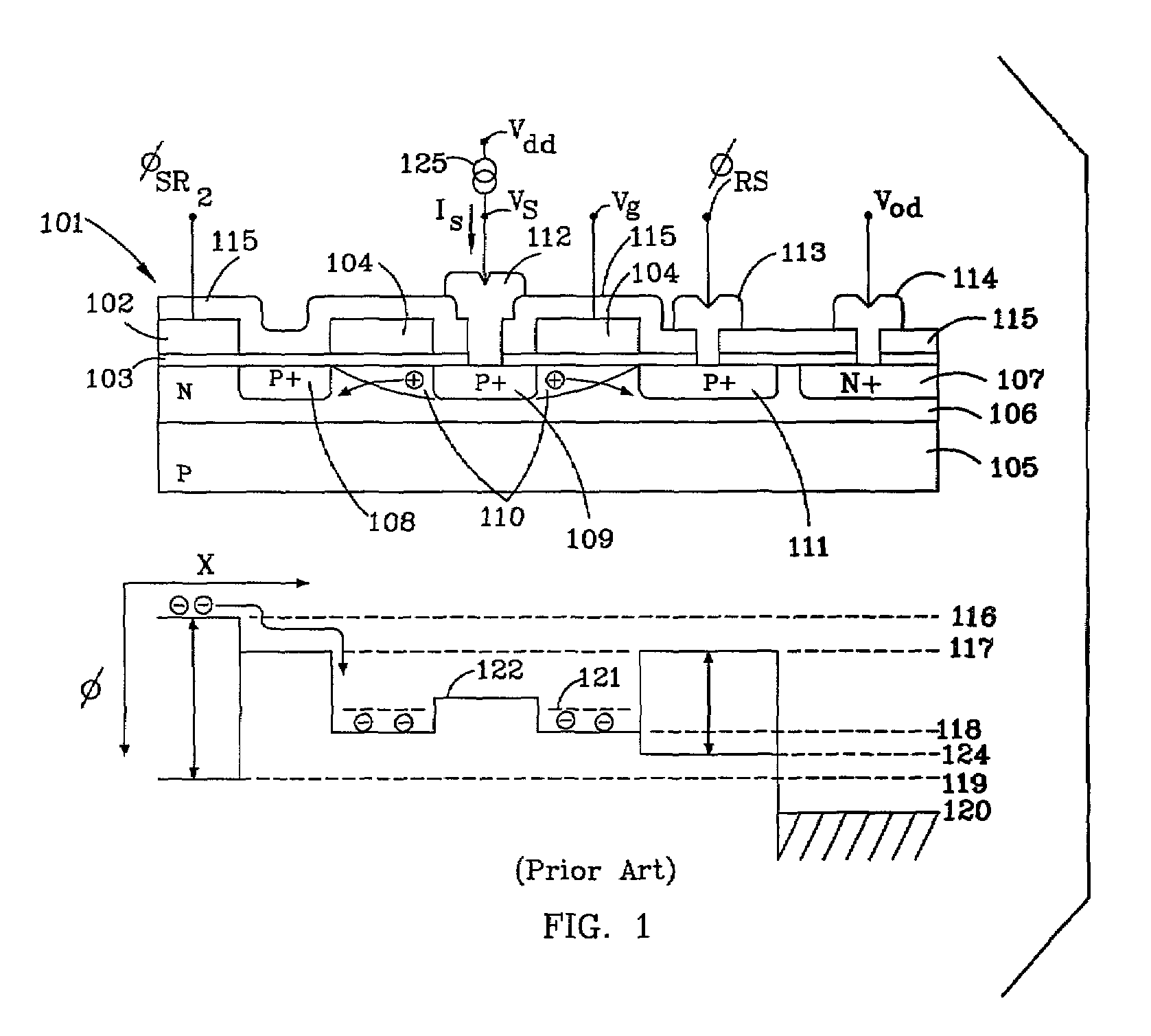
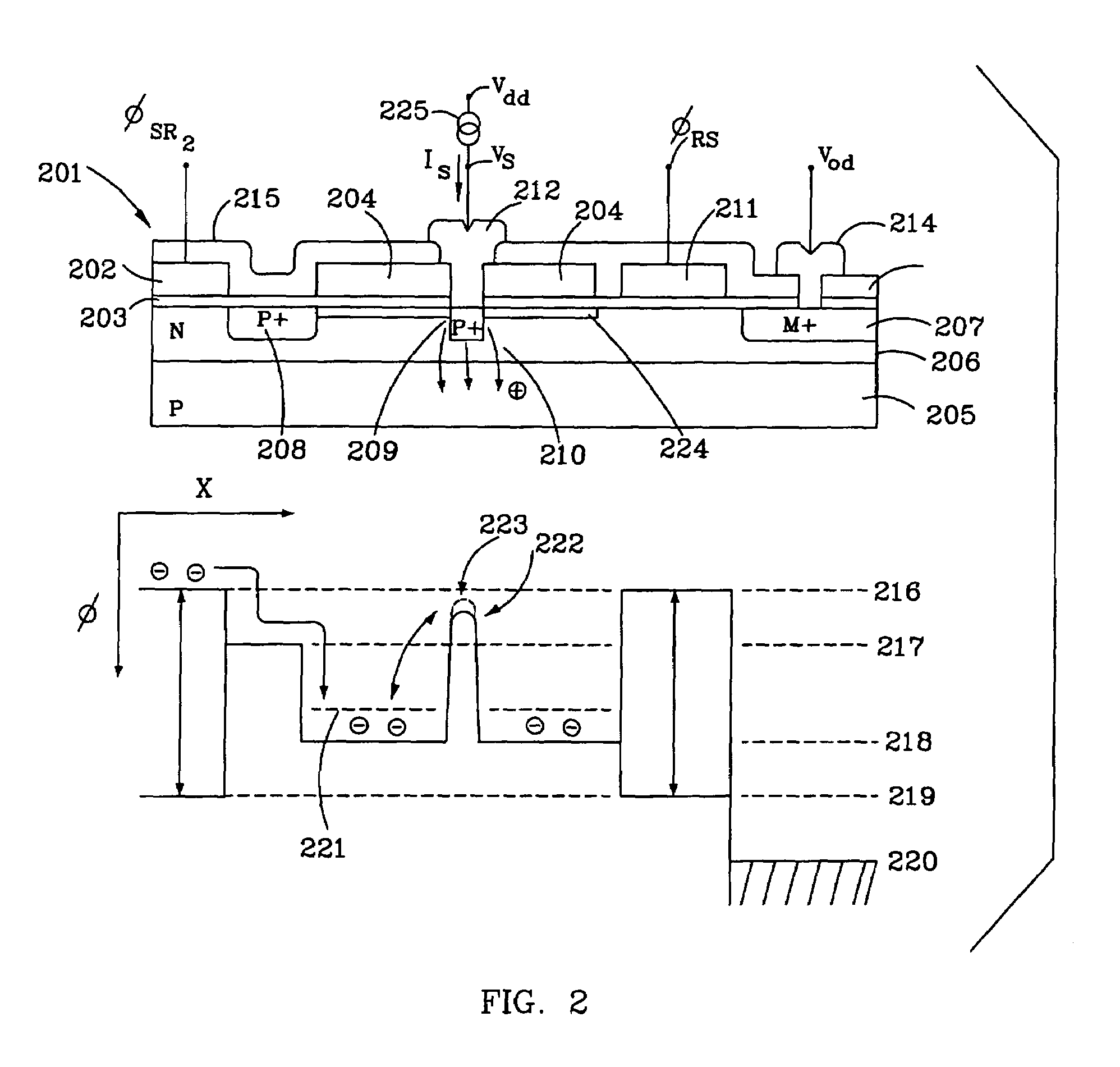
[0014]In FIG. 1, a cross section 101 of the typical prior art BCD charge detection node is shown together with the corresponding potential profiles. The p-type doped substrate is indicated as the region 105 that includes an n-type doped buried channel 106 near its surface. Additional p+ type doped regions 108, 109, and 111 have been diffused or implanted into the structure as shown in FIG. 1. The n+ type doped region 107 serves as the output diode that collects charge after sensing and reset. A suitable dielectric layer 103, for example silicon dioxide, separates the substrate from gates 102 and 104. Another dielectric layer 115 may be deposited over the structure to provide the necessary isolation before metal interconnects 112, 113, and 114 are formed. The gate 104 has a doughnut shape and completely surrounds the region 109 that serves as source of the p channel MOS transistor. The drain of this transistor is also circular in shape and is formed by regions 108, 111 and by channel...


PUM


Abstract

A charge detection system used in an image sensor consists of the vertical punch through transistor with the gate surrounding its source and connected to it. The charge detector has a large conversion gain, high dynamic range, low reset feed through, and low noise. It senses charge nondestructively, which avoids generation of kTC noise. Additional embodiments of the invention include a standard reset gate option, a resistive reset gate option, and a lateral punch through transistor reset option to minimize the reset feed through. The charge detection system can be used in all know CCD image sensor architectures as well as in most CMOS image sensor architectures.

Description

PRIORITY[0001]Priority is claimed from Provisional application Ser. No. 60 / 245,942, filed Nov. 6, 2000.FIELD OF THE INVENTION[0002]The present invention relates to solid-state image sensors, and more particularly to charge detection amplifiers of image sensors that employ a vertical punch through transistor for sensing charge.BACKGROUND OF THE INVENTION[0003]A typical image sensor senses light by converting impinging photons into electrons that are integrated (collected) in the sensor pixels. After the integration cycle is completed, charge is converted into a voltage that is supplied to the output terminals of the sensor. The charge to voltage conversion is accomplished either directly in the sensor pixels, such as in the Active Pixel CMOS image sensors, or remotely off the sensing area, in charge conversion amplifiers. The key element of every charge conversion amplifier is the charge detection node. As charge is transferred onto the node, its potential changes in proportion to th...

Claims


Application Information

Patent Timeline
IPC IPC(8): H04N3/14H01L27/00H01L27/148H01L27/146
CPCH01L27/14609H01L27/14812H01L27/14636
Inventor HYNECEK, JAROSLAV
Owner ISETEX
Why Eureka
Try Eureka