Fast high-swing modulator driver circuit

a driver circuit and high-swing technology, applied in the field of electronic modulator driver circuits, can solve the problems of adding to the complexity of the system, and distortion significantly affecting the bit-error rate and thus the usable distance of the fiber optic link,

Active Publication Date: 2005-07-07
MARVELL ASIA PTE LTD
View PDF0 Cites 33 Cited by
  • Summary
  • Abstract
  • Description
  • Claims
  • Application Information

AI Technical Summary

Benefits of technology

[0012] When so arranged, the output stage amplifies an input signal applied to the first transistor's base, and provides the amplified signal at the driver circuit's output. Grounding the first transistor's collector and AC-coupling the second transistor's base to ground eliminates the Miller effects which would otherwise degrade the stage's speed. In addition, the second transistor's common-base configuration provides a higher breakdown voltage than prior art common-emitter output stages, without the higher supply voltage and the stacked devices found in the prior art cascode approach. Thus, the stage is capable of operating at high speeds with a large output voltage swing, making it well-suited for providing the 6-8 volt p-p, 10 Gb / s driving voltage required by an electro-optical modulator such as a single-ended Mach-Zehnder.

Problems solved by technology

The dual-drive modulator uses less voltage per input, but its two input signals require precise amplitude and phase matching which adds to system complexity.
The modulator also transfers any variation or imperfection in the amplified electrical waveform directly to the optical signal, and this distortion significantly affects the bit-error rate and thus the usable distance of the fiber optic link.
These factors make the circuit design of the modulator driver especially critical.
The fundamental problem in MZ modulator driver design is obtaining high bandwidth (fast rise and fall times) with high pulse fidelity (damped response and low jitter) while using transistors large enough to handle the high voltage and current required to drive typical 50-ohm MZ modulators.
This increases the circuit's bandwidth, but also greatly expands its physical size and results in limited integrability with other circuits.
Moreover, TWA-based drivers have low electrical gain since they basically comprise a single (albeit large) transistor.
The disadvantage of PHEMT devices is that their varying threshold voltage and conductance characteristics make them inappropriate for creating either high-precision analog or low-power digital control circuits.
These external circuits add considerable cost and complexity to the system.
These capacitances, multiplied by the Miller effect that arises due to the inverting voltage gain in this common-emitter configuration, tend to reduce the stage's bandwidth and cause unacceptably slow rise time.
This capacitance also degrades the output return loss of the driver, which leads to jitter when operating with an impedance-mismatched load.
However, this approach requires the use of four large devices, which can make the circuit layout difficult.
In addition, the stacked transistors require a higher supply voltage, and thus the circuit consumes more DC power.

Method used


Image

  • Fast high-swing modulator driver circuit
  • Fast high-swing modulator driver circuit
  • Fast high-swing modulator driver circuit

Examples


Embodiment Construction

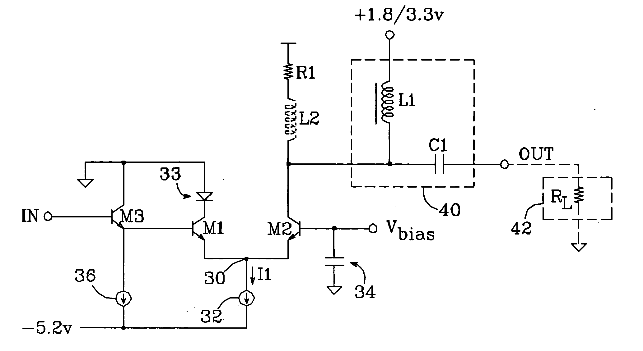
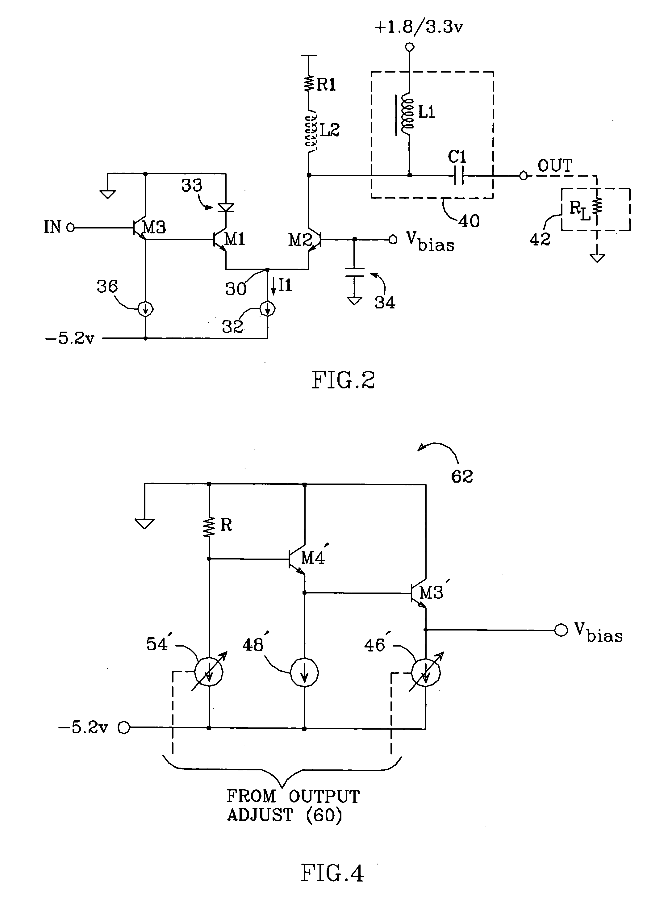
[0023] The present invention is a driver circuit which includes an output stage capable of delivering a large output voltage swing at high speeds, making the driver circuit particularly well-suited for driving certain electro-optical modulators. The basic principles of a driver circuit in accordance with the present invention are illustrated in the schematic shown in FIG. 2. A circuit's output stage comprises a pair of bipolar transistors M1 and M2 arranged as a differential pair, with their emitters connected together at a common node 30 and a current source 32 connected between node 30 and a supply voltage (−5.2 volts in the example shown, though other voltages could also be used) which provides a bias current I1 to the differential pair. The base of transistor M1 provides an input terminal for the stage, and the collector of M2 provides the driver circuit's output The collector of input transistor M1 is coupled to ground, preferably via a diode 33 which serves to reduce the power...


PUM

PropertyMeasurementUnit
currentaaaaaaaaaa
resistanceaaaaaaaaaa
drive voltageaaaaaaaaaa

Abstract

A fast, high-swing driver circuit for driving an electro-optical modulator includes an output stage comprising first and second transistors arranged as a differential pair. The collector of the first transistor is coupled to ground, and its base provides the stage's input. The collector of the second transistor is coupled via an impedance to a supply voltage, and provides the stage's output. A reference voltage is provided to the second transistor's base, which is also AC-coupled to ground. A bias generator provides the second transistor's base voltage, and a second differential pair converts a differential input signal to a single-ended output that drives the output stage's input—preferably via a pair of cascaded emitter-follower stages that serve to present a low impedance. A complete electro-optical modulator driver is formed with the addition of a bias-T network at the output stage's output.

Description

BACKGROUND OF THE INVENTION [0001] 1. Field of the Invention [0002] This invention relates to the field of electro-optical modulator driver circuits, and particularly to modulator driver circuits requiring a high output voltage swing and high speed. [0003] 2. Description of the Related Art [0004] Fiber optic cables are often driven by means of a continuous laser modulated by an electro-optical modulator. One such modulator that is often used in high-bit-rate (˜10 Gb / s or more) communication systems is the Mach-Zehnder (MZ) modulator. MZ modulators use an optical interferometer fabricated in nonlinear material—e.g. Lithium Niobate, in which the velocity of light can be varied by an applied, electric field—to either block or transmit laser light as a function of an externally applied driving voltage. This voltage is either applied to a single input (“single-ended” drive) or is applied differentially at two inputs (in a “dual-drive” MZ modulator). The dual-drive modulator uses less vol...

Claims


Application Information

Patent Timeline
Patent Type & Authority Applications(United States)
IPC IPC(8): G02F1/01H01S3/00H01S3/10H01S5/042
CPCH01S5/0427G02F1/0121
Inventor POBANZ, CARL W.
Owner MARVELL ASIA PTE LTD
Why Eureka
Try Eureka