Semiconductor device having memory and logic devices with reduced resistance and leakage current

a technology of logic devices and semiconductors, applied in semiconductor devices, capacitors, electrical devices, etc., can solve the problems of reducing the operating speed of logic devices, increasing the leakage current of capacitors electrically connected to source/drain regions, and deteriorating data storage characteristics of drams, so as to reduce the resistance and reduce the leakage current of capacitors.

Active Publication Date: 2006-07-18
RENESAS ELECTRONICS CORP
View PDF6 Cites 19 Cited by
  • Summary
  • Abstract
  • Description
  • Claims
  • Application Information

AI Technical Summary

Benefits of technology

[0007]An object of the present invention is to provide a semiconductor technique that can achieve both of lowered resistance in a region where a logic device is formed and reduced leakage current of the capacitor of a memory device.
[0009]The first silicide film in the memory formation region is thinner than the second silicide film in the logic formation region, so that the leakage current between the first and third impurity regions is lower than the leakage current between the second and fourth impurity regions. On the other hand, since the second silicide film is thicker than the first silicide film, the resistance of the fourth impurity region is lower than that of the third impurity region. Thus it is possible to achieve both of lowered resistance of the fourth impurity region in the logic formation region and reduced leakage current of the capacitor electrically connected to the first silicide film.
[0011]Since the first gate aspect ratio is larger than the second gate aspect ratio, the use of the nondirectional sputtering method in step (e) causes the metal material to form thinner on the third impurity region than on the fourth impurity region. This causes in step (f) the silicide film to form thinner in the upper surface of the third impurity region than in the upper surface of the fourth impurity region. This makes the leakage current between the first and third impurity regions lower than the leakage current between the second and fourth impurity regions. On the other hand, since the silicide film in the upper surface of the fourth impurity region is thicker than the silicide film in the upper surface of the third impurity region, the fourth impurity region presents a lower resistance than the third impurity region. Thus it is possible to achieve both of lowered resistance of the fourth impurity region in the logic formation region and reduced leakage current of the capacitor electrically connected to the first silicide film.

Problems solved by technology

Therefore, when the silicide film in the logic portion is formed thick to achieve higher speed of the logic device, then the silicide film in the DRAM portion, too, forms thick, which increases the leakage current of capacitors electrically connected to the source / drain regions.
This deteriorates data storage characteristic of the DRAM.
On the other hand, when the silicide film in the DRAM portion is formed thin to reduce the capacitor leakage current, then the silicide film in the logic portion also forms thin, which lowers operating speed of the logic device.

Method used


Image

  • Semiconductor device having memory and logic devices with reduced resistance and leakage current
  • Semiconductor device having memory and logic devices with reduced resistance and leakage current
  • Semiconductor device having memory and logic devices with reduced resistance and leakage current

Examples


first preferred embodiment

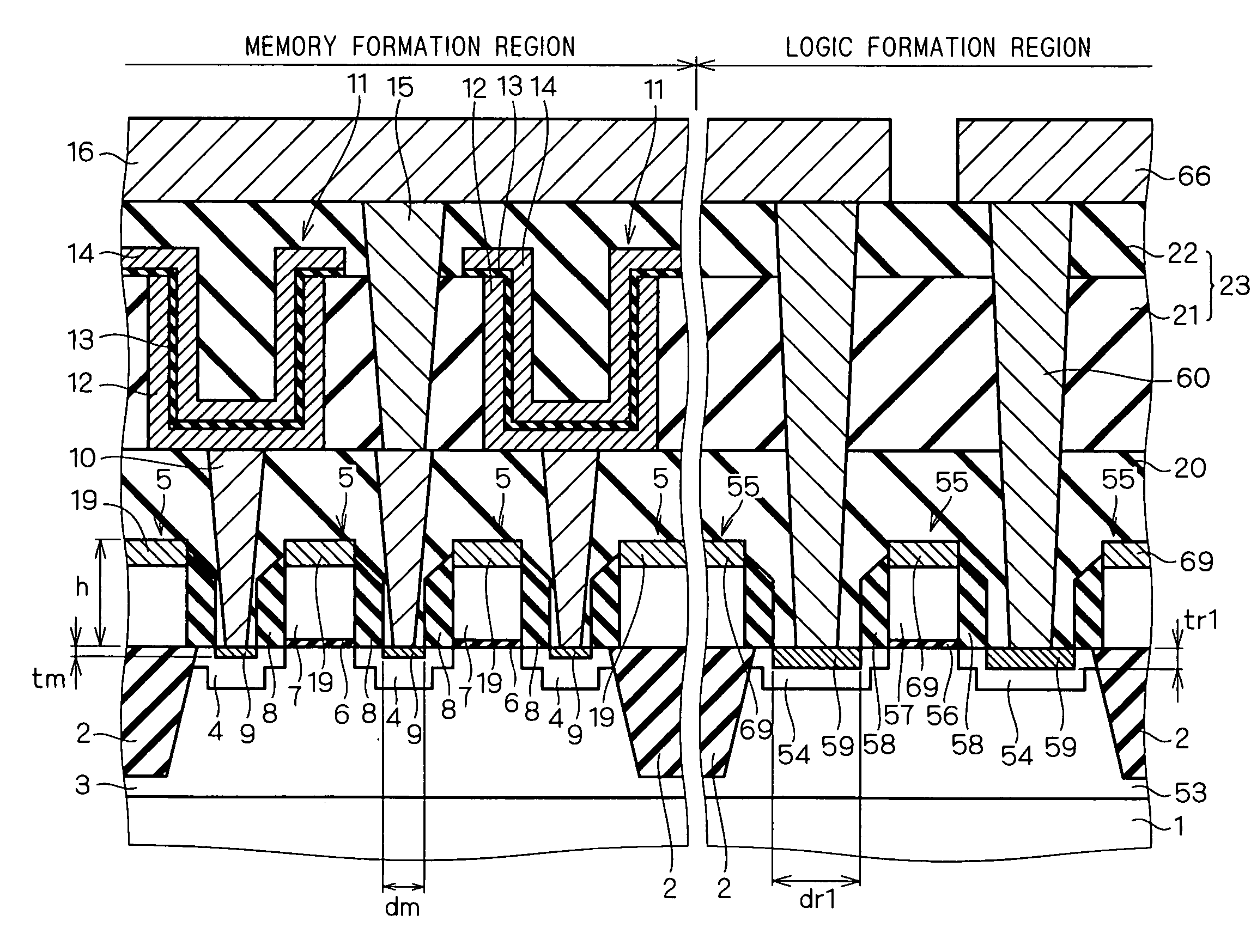
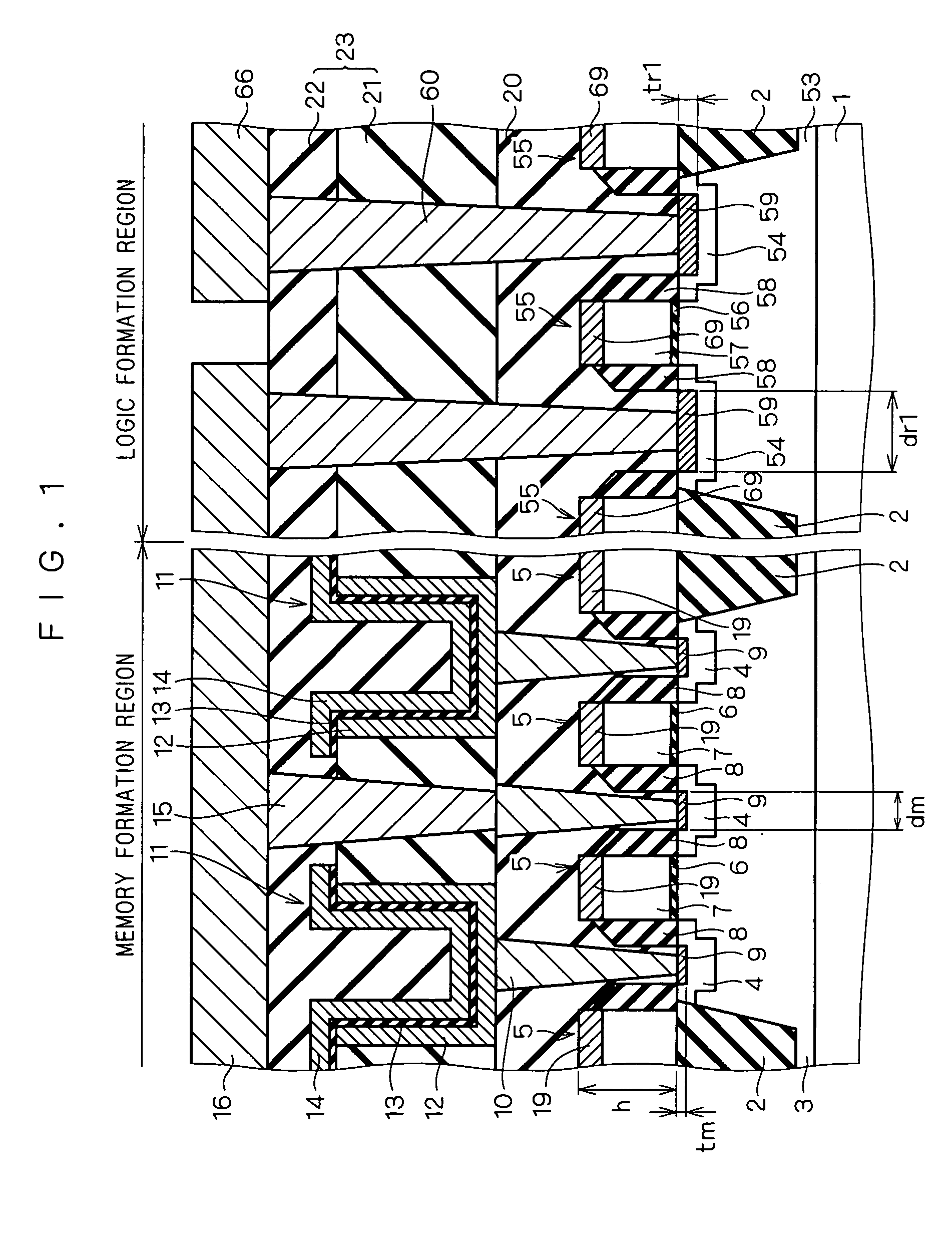
[0018]FIG. 1 is a cross-sectional view showing the structure of a semiconductor device according to a first preferred embodiment of the invention. The semiconductor device of the first preferred embodiment is a memory / logic mixed semiconductor device, where DRAM having CUB (Capacitor Under Bit line) structure memory cells is adopted as the memory device and Dual-Gate salicide CMOS transistors are adopted as the logic device, for example.

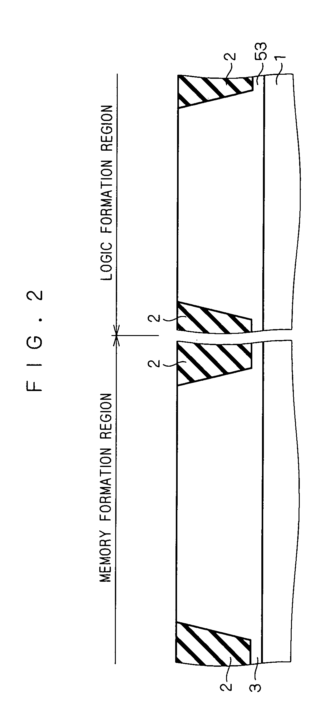
[0019]As shown in FIG. 1, the semiconductor device of the first preferred embodiment has a semiconductor substrate 1 that is, for example, an n-type silicon substrate. Element isolation insulating films 2 are formed in the upper surface of the semiconductor substrate 1 to divide the semiconductor substrate 1 into a plurality of regions.

[0020]In a region where the memory device is formed (hereinafter referred to as a “memory formation region”), a p-type well region 3 is formed in the upper surface of the semiconductor substrate 1. In a region where th...

second preferred embodiment

[0062]FIG. 9 is a cross-sectional view showing the structure of a semiconductor device according to a second preferred embodiment of the invention. According to the second preferred embodiment, basically, the semiconductor device as shown in the first preferred embodiment further includes, in the logic formation region, a region having a gate aspect ratio that is larger than the second gate aspect ratio. In the second preferred embodiment, the region having the second gate aspect ratio described in the first preferred embodiment is referred to as a “first region” and the region having a gate aspect ratio larger than the second gate aspect ratio, an additional region introduced in the second preferred embodiment, is referred to as a “second region.”

[0063]As shown in FIG. 9, the semiconductor device of the second preferred embodiment has a well region 83, or a p-type impurity region, that is formed in the second region of the logic formation region in the upper surface of the semicond...


PUM


Abstract

A semiconductor technique is provided which can achieve both of lowered resistance in a logic formation region and reduced leakage current of the capacitor of a memory device. Source / drain regions (4) are formed in the upper surface of a semiconductor substrate (1) in a memory formation region and cobalt silicide films (9) are formed in the upper surfaces of the source / drain regions (4). Source / drain regions (54) are formed in the upper surface of the semiconductor substrate (1) in a logic formation region and cobalt silicide films (59) are formed in the upper surfaces of the source / drain regions (54). The cobalt silicide films (59) in the logic formation region are thicker than the cobalt silicide films (9) in the memory formation region.

Description

BACKGROUND OF THE INVENTION[0001]1. Field of the Invention[0002]The present invention relates to a memory / logic mixed semiconductor device in which memory and logic devices are fabricated on a semiconductor substrate, and to a method for manufacturing the same.[0003]2. Description of the Background Art[0004]In the field of recent system LSIs, memory / logic mixed semiconductor devices are attracting attention in which large-capacity high-speed memory devices and logic devices are constructed on the same semiconductor substrate. Among them, as to semiconductor devices mounted with DRAMs suitable for large capacity applications, devices in which silicide films are formed within memory cells are developed to achieve higher speed memory devices.[0005]Japanese Patent Application Laid-Open No. 2001-127270 (hereinafter referred to as a first patent document) discloses an example of such a memory / logic mixed semiconductor device having silicide films within memory cells. According to the tech...

Claims


Application Information

Patent Timeline
Patent Type & Authority Patents(United States)
IPC IPC(8): H01L29/76H01L21/28H01L21/02H01L21/8239H01L21/8242H01L27/108
CPCH01L27/10811H01L27/10852H01L27/1052H01L27/10897H01L28/91H01L29/66477H01L27/10894H01L21/28518H10B12/312H10B99/00H10B12/50H10B12/09H10B12/033
Inventor SHINKAWATA, HIROKI
Owner RENESAS ELECTRONICS CORP
Why Eureka
Try Eureka