Scatterometry and acoustic based active control of thin film deposition process

Inactive Publication Date: 2006-07-18
GLOBALFOUNDRIES INC
View PDF22 Cites 16 Cited by
  • Summary
  • Abstract
  • Description
  • Claims
  • Application Information

AI Technical Summary

Benefits of technology

[0012]One or more deposition components may be employed in fabricating a particular chip. It is to be appreciated by one skilled in the art that any suitable deposition components may be employed with the present invention. For example, deposition components including, but not limited to various types of chemical vapor deposition (CVD) components (e.g., LPCVD, MOCVD, ALCVD, etc.) and/or plasma enhanced chemical vapor deposition (PECVD) components may be employed in accordance with the present invention. The deposition components are selectively driven by the system to deposit a thin film to a desired thickness and/or uniformity within an acceptable level of defects and/or impurities. It is important to deposit enough thin film on a wafer to achieve the desired properties, therefore the thickness or amount of thin film deposited must be considered. As the non-uniformity of the thin film layer increases, performance and speed of the device decreases. Thus, controlling the deposition components such as thickness, uniformity, and acceptable levels of defects and/or impurities facilitates achieving faster and higher density devices.
[0013]The present invention operates by comparing signatures generated by light reflected by the thin film to desired signatures. By comparing desired signatures to measured signatures, runtime feedback may be employed to more precisely control the thin film deposition, and to identify and reject wafers upon which a thin film has been deposited with unacceptable levels of defects and/or impurities. Alternatively, or in addition, acoustic techniques may also be used as described above. As a result, higher quality monitoring and controlling of thin film deposition is achieved, which in turn increases performance and yield of the chip.
[0014]In accordance with one aspect of the present invention, a system for controlling a thin film deposition process is provided, the system comprising: one or more thin film deposition components operative to deposit a thin film on one or more portions of a wafer; a thin film deposition component driving system for driving the one or more deposition components; a system for directing light on to the wafer; a monitoring system adapted to detect structural irregularities associated with the deposited thin film by comparing reflected light data with a database comprising known thin film reflected light signatures; and a processor operatively coupled to the monitoring system and the thin film

Problems solved by technology

Further, selectively marking wafers for further processing and/or rejection when a thin film has a

Method used


Image

  • Scatterometry and acoustic based active control of thin film deposition process
  • Scatterometry and acoustic based active control of thin film deposition process
  • Scatterometry and acoustic based active control of thin film deposition process

Examples


Embodiment Construction

[0041]The present invention will now be described with reference to the drawings, wherein like reference numerals are used to refer to like elements throughout. The following detailed description is of the best modes presently contemplated by the inventors for practicing the invention. It should be understood that the description of these aspects are merely illustrative and that they should not be taken in a limiting sense.

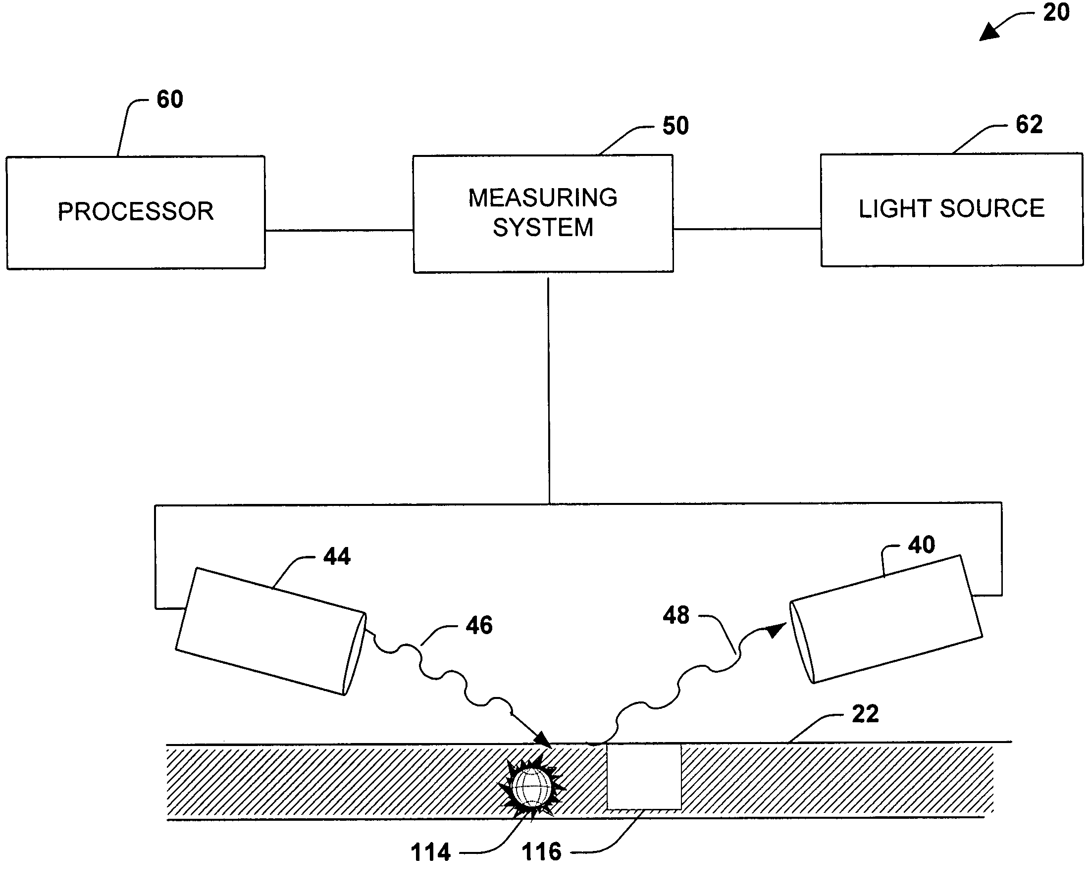
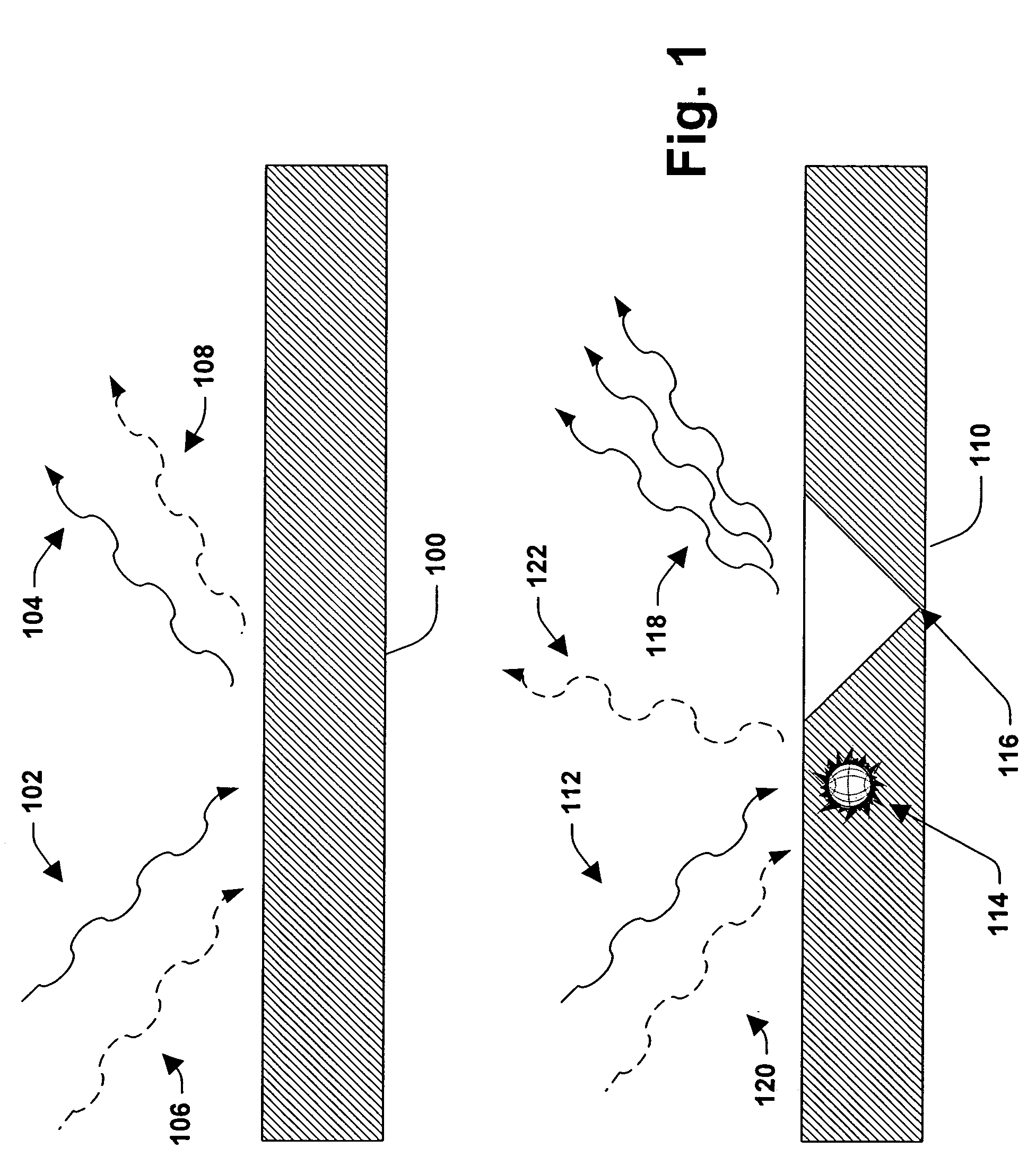
[0042]Referring initially to FIG. 1, two types of exemplary deposited thin films are shown. FIG. 1 shows a thin film 100, having substantially no imperfections, being subjected to a scatterometry based monitoring system. The monitoring system will be described in greater detail later. One or more beams of light 102 are directed at the thin film 100 and are reflected off the thin film as reflected light 104. Relationships including, but not limited to, an angle of incidence of the light 102 with the thin film 100, an angle of reflection of the reflected waves 104 a...


PUM


Abstract

A system for monitoring and controlling the deposition of thin films employed in semiconductor fabrication is provided. The system includes one or more acoustic and/or ultrasonic wave sources, each source directing waves onto one or more thin films deposited on a wafer. Waves reflected from the thin film is collected by a monitoring system, which processes the collected waves. Waves passing through the thin film may similarly be collected by the monitoring system, which processes the collected waves. The collected waves are indicative of the presence of impurities and/or defects in the deposited thin film. The monitoring system analyzes and provides the collected wave data to a processor, which determines whether adjustments to thin film deposition parameters are needed. The system also includes a plurality of thin film deposition devices associated with depositing thin films on the wafer. The processor selectively controls thin film deposition parameters and devices to facilitate regulating deposition.

Description

TECHNICAL FIELD[0001]The present invention generally relates to semiconductor processing, and in particular to a system for monitoring and controlling thin film deposition.BACKGROUND[0002]In the semiconductor industry, there is a continuing trend toward higher device densities. To achieve these high densities there have been, and continue to be, efforts toward scaling down device dimensions (e.g., at sub-micron levels) on semiconductor wafers. In order to accomplish such high device packing densities, smaller feature sizes and more precise feature shapes are required. This may include the width, thickness and spacing of interconnecting lines, spacing and diameter of contact holes, and the surface geometry, such as corners and edges, of various features.[0003]The requirement of small features with close spacing between adjacent features requires sophisticated manufacturing techniques to ensure that quality and operability of the features are not compromised for the purpose of reducin...

Claims


Application Information

Patent Timeline
IPC IPC(8): G01B11/02G01B15/02
CPCG01B11/0625G01B11/0683G01B17/025G01N21/94G01N21/8422G01N21/88G01N21/47
Inventor HALLIYAL, ARVINDSINGH, BHANWARSUBRAMANIAN, RAMKUMAR
Owner GLOBALFOUNDRIES INC
Why Eureka
Try Eureka