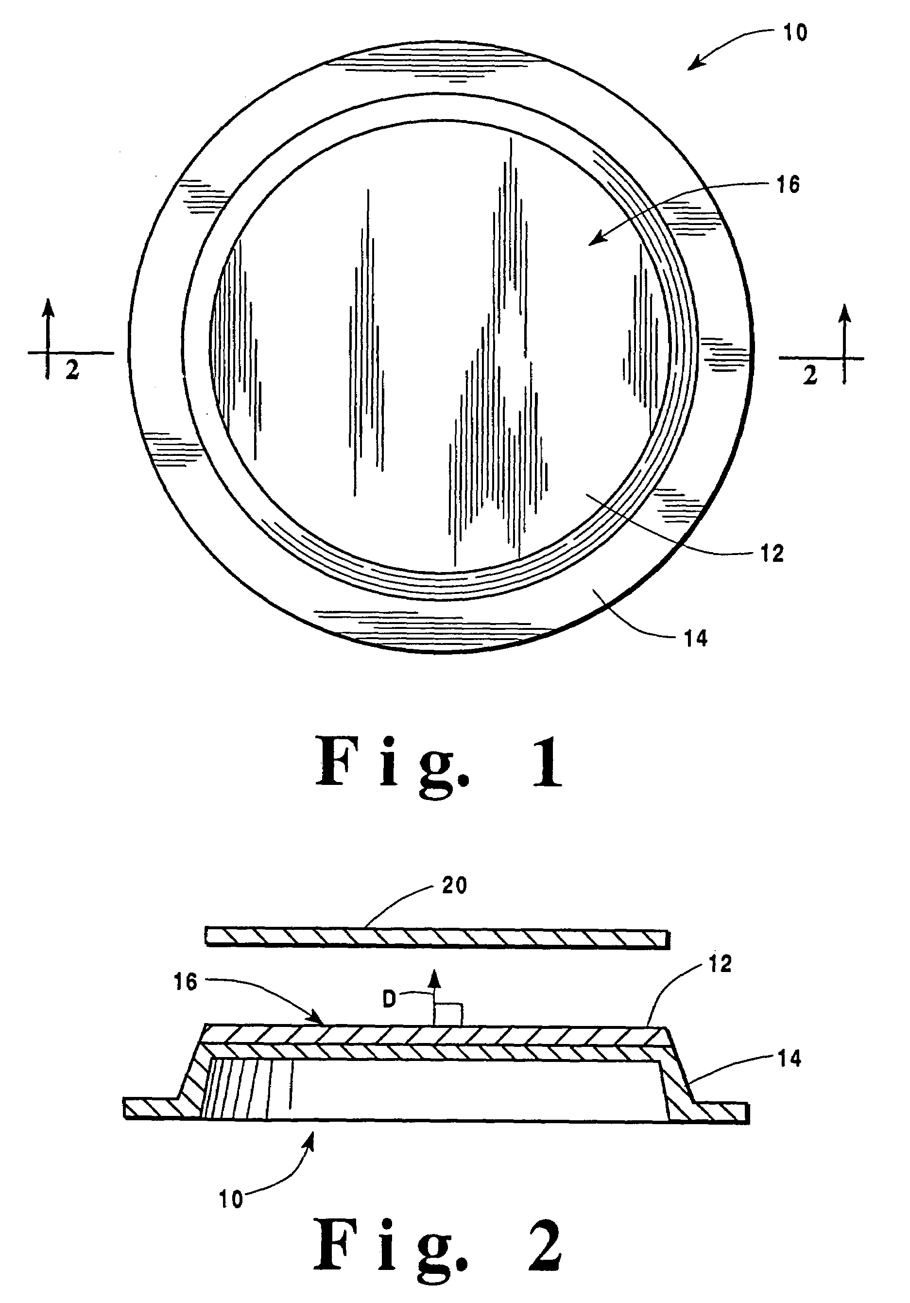
Textured-grain-powder metallurgy tantalum sputter target
a technology of powder metallurgy and tantalum sputter, which is applied in the direction of diaphragms, metallic material coating processes, electrical equipment, etc., can solve the problems of manufacturers reducing the yield of the sputter, and increasing the thickness of the sputter. achieve the effect of increasing the uniformity of the sputter
- Summary
- Abstract
- Description
- Claims
- Application Information
AI Technical Summary
Benefits of technology
Problems solved by technology
Method used
Image
Examples
example 1
[0016]The following table summarizes preliminary experiments conducted in a 603 batch sputter system manufactured by MRC with 4″ (10 cm) diameter targets. Sputter testing in this system was conducted at a power of 640 W for up to 15 kWh, a wafer scan speed of 16 cm / min corresponding to a film thickness of 1000 Å, a chamber pressure of 10 mTorr, and a target-to-wafer spacing of 2.0 inches (5.1 cm). The sheet resistance was measured at 9 points on silicon oxide wafers having a diameter of 75 mm with a 6 mm edge exclusion.
[0017]For purposes of this specification lettered targets represent comparative examples and numbered targets represent examples of the invention. Although the sputter conditions were not optimized, all experiments were conducted under identical conditions and therefore allowed a comparison between a cast and thermomechanically processed reference target (Target A) and various powder metallurgy targets (Targets B to G and 1). Orientation ratios contained in the Exampl...
example 2
[0020]The powder metallurgy RMX-12 sputter targets exhibited an average grain size of 40 to 50 microns and a high (222) crystallographic orientation ratio.
[0021]Sputter testing in the Eclipse system was conducted at a power of 10 kW for up to 50 kWh, a deposition time of 60 seconds, an argon flow rate of 100 sccm, a chamber pressure of 15 mTorr, a wafer temperature of 150° C., and a target-to-wafer spacing of 2.5 inches (6.4 cm). The sheet resistance was measured at 49 points on silicon oxide wafers having a diameter of 150 mm with a 6 mm edge exclusion.
[0022]Table 2 summarizes grain orientation data of a conventional target manufactured by casting and thermomechanical processing (Target G) and two powder metallurgy targets with forging (Target 2) and without forging (Target 3).
[0023]
TABLE 2Grain Orientation Ratio (Percent)Cast / PressedP / M TargetP / M TargetGrainTarget(Forged)(Not Forged)OrientationG23(110)3011(200)192020(211)151010(310)1699(222)206060(200)–(222)YesNoNoBanding
[0024]Tab...
PUM
| Property | Measurement | Unit |
|---|---|---|
| Fraction | aaaaa | aaaaa |
| Fraction | aaaaa | aaaaa |
| Fraction | aaaaa | aaaaa |
Abstract
Description
Claims
Application Information
