Method of identifying and analyzing semiconductor chip defects

a technology of semiconductor chips and defects, applied in the field of identifying and analyzing semiconductor chip defects, can solve problems such as difficulty in understanding the defect data obtained by the drt instrument, complex defect data obtained using these instruments, and problems such as difficulty in identifying chip defect causes based on defect composition, etc., to achieve the effect of being easily analyzed

Inactive Publication Date: 2006-07-25
SAMSUNG ELECTRONICS CO LTD
View PDF19 Cites 7 Cited by
  • Summary
  • Abstract
  • Description
  • Claims
  • Application Information

AI Technical Summary

Benefits of technology

[0019]To overcome the foregoing problems, various preferred embodiments of the present invention provide an improved map of wafer defects, defect cause distribution charts, and a method of analyzing the causes of defects simply and quickly.
[0020]In a preferred embodiment of the present invention, a method of identifying and marking chip defects based on the cause of the defect is provided. Defects are first identified using a semiconductor defect inspection instrument. The defect inspection instrument is then used to analyze the composition of the defect to determine a cause thereof. The defects are thereafter marked on a wafer map using the same marks to represent defects caused in the same manner. Using these specially-coded markings, graphs and other charts can then be prepared to display distributions, skews, and other arrangements of defect characteristics. The defects can then be more readily analyzed statistically.

Problems solved by technology

Unfortunately, even though these newly introduced DRT instruments that analyze defects based on composition have already helped obtain cleanness levels of Class 1, problems have been encountered in identifying chip defect causes based on defect composition.
In particular, defect data obtained using these instruments is complicated.
Anyone other than a highly trained specialist therefore has difficulty understanding the defect data obtained by the DRT instrument.
A mass production implementation of these DRT instruments is therefore impractical without better analysis tools.
Defect management in mass production of semiconductor products is critical because defects are directly related to mass production yields.
Defect classifications using these tools, however, remain in a primitive state and can include numerous operator errors.
These errors impede the recent trend toward miniaturization of semiconductor devices.
In addition, even though some analysis is typically performed to help eliminate defects, it is difficult to correctly classify and analyze defects according to type using the prior art classification methods.
Furthermore, despite the amount of information obtained, that information alone is not sufficient to determine the cause of individual defects.
In other words, even though statistical classification and management of the defects is possible, using the information obtained, the information regarding individual defects is not sufficient to determine the cause of that defect.
However, the data obtained from the conventional component analysis is difficult to understand and requires careful review by a skilled technician.
The defects generated on a chip have a significant influence on the yield loss and on the inferiority of chip characteristics.
It should be noted, however, that even when there are a hundred chips containing defects, the yield loss is generated in only between about 1 to 30 of those chips (i.e., about 1-30% of the chips having defects).
For example, a DRAM device chip cannot be produced when a defect exists in an area surrounding a memory cell.
When the defect exists within the memory cell, however, the chip can still be used to produce a good chip.
Defects in manufacturing processes, such as a photolithography process, an etching process, a diffusion process, an ion implanting process, and a thin film deposition process, can also result in chip failure.
It is therefore often difficult to clearly identify the influence of chip defects on yield loss.
As described above, the degree of yield loss resulting from chip defects varies depending on the type of device being manufactured and the processes used to produce that device.
In addition, the conditions in a semiconductor manufacturing plant, such as the equipment, surroundings, and treatments can also cause defects.
Managing yield by managing defects is therefore extremely difficult.
The yield loss and the particular defect ratios are increased when the total number of defects and the total number of defect chips are increased.
Because subsequent semiconductor processes can vary the yield loss in the produced semiconductor device, it is difficult to precisely determine at this stage how the defects will influence the ultimate yield loss.
It is therefore also impractical to measure absolute values of the yield loss by the defects.
The method described in that application, however, can only properly manage and correctly measure the number of chips with defects in a unit process or between unit processes.
Information for each of the defects is insufficient to enable the desired analysis and a quick response to the chip defects is therefore difficult.

Method used


Image

  • Method of identifying and analyzing semiconductor chip defects
  • Method of identifying and analyzing semiconductor chip defects
  • Method of identifying and analyzing semiconductor chip defects

Examples


Embodiment Construction

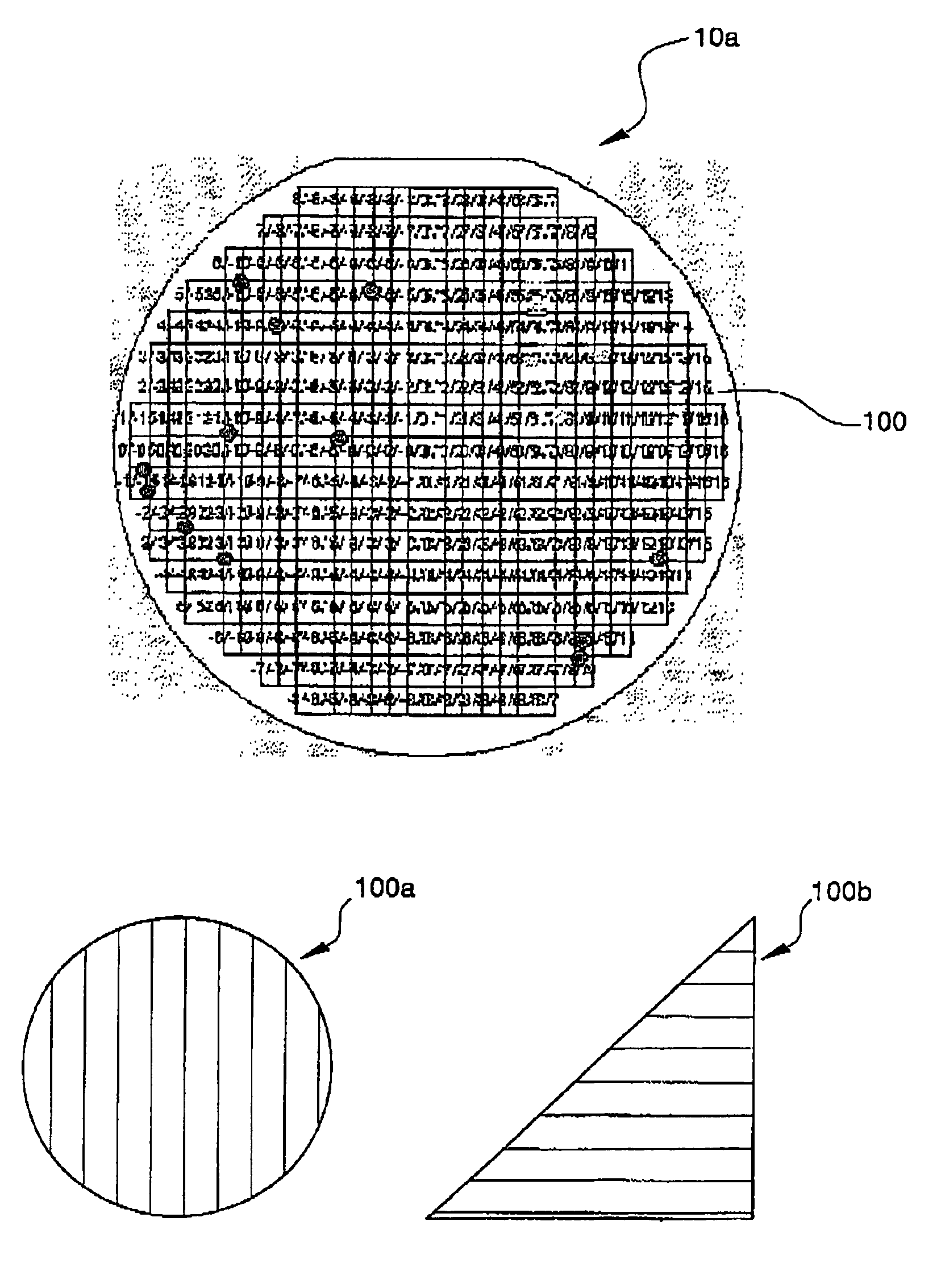
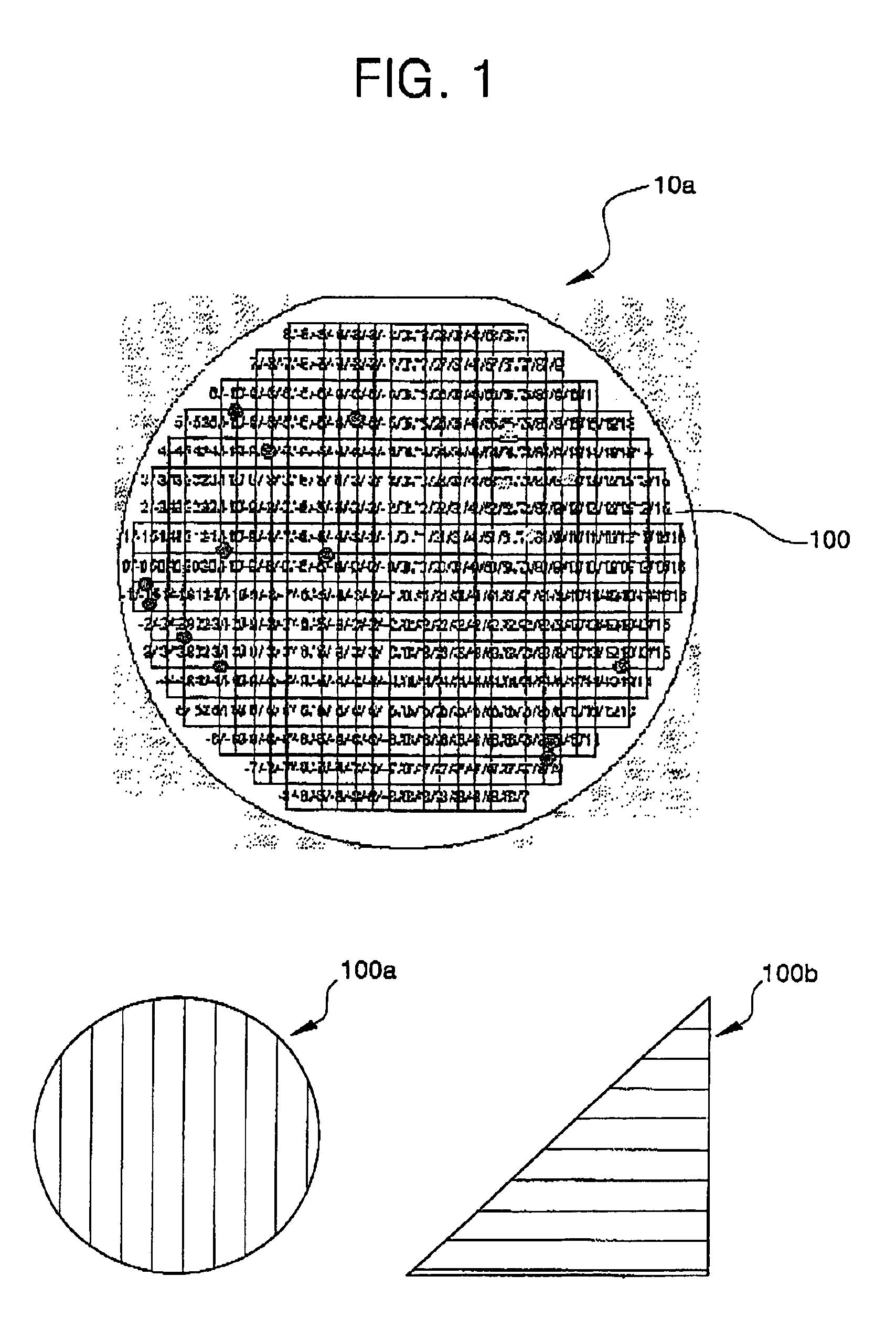
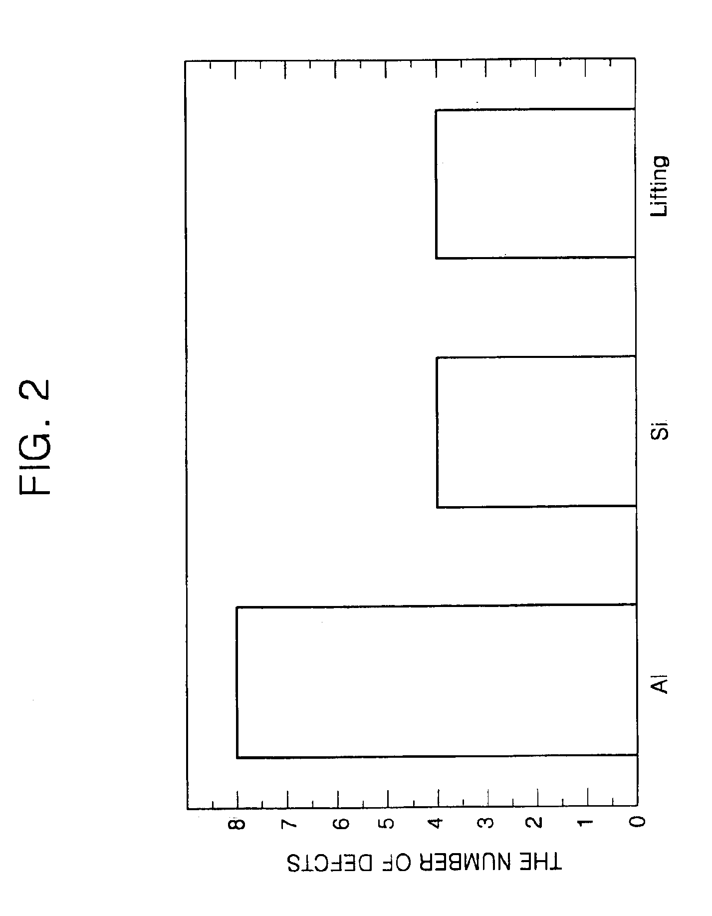
[0027]Various preferred embodiments of the present invention will now be described in further detail. Referring to FIG. 1, a wafer defect map 10a, according to one aspect of the present invention, identifies the location of defects on the wafer using markings 100. In the wafer defect map of FIG. 1, like markings are used to represent defects of the same type. FIG. 2 is a bar graph illustrating a process of classifying the defects according to another aspect of the present invention.

[0028]Referring to FIGS. 1 and 2, a method of identifying and analyzing defects in semiconductor chips, according to a preferred aspect of this invention, will be described. One or more semiconductor defect inspection instruments are first used to identify the location and type of defects on a wafer. A Defect Review Tool (DRT), such as the KLA SEM, can be used for this purpose. After the defects have been located, the same defect inspection instrument, or a different inspection instrument, is used to dete...


PUM


Abstract

According to a preferred aspect of this invention, locations of defects on a semiconductor wafer are found using semiconductor defect inspection instrumentation. Defect composition can also be determined using inspection instrumentation. Wafer defects are represented on a wafer defect map using markings wherein locations of the markings on the map correspond to the locations of the defects on the wafer. The markings also preferably represent a defect type and/or composition. Color-coded dots, for instance, can be used to represent like defect causes or types with like colors. Graphs can be prepared to display defect characteristics using distributions and skews to facilitate quick statistical analysis of the defects. In this manner, wafer defects can be analyzed quickly and efficiently based on characteristics thereof, including, for example, defect type, composition, and cause. This information can be used to help prevent future defects during mass production, thereby improving yield.

Description

CROSS REFERENCE[0001]This application claims priority, under 35 U.S.C. § 119, from Korean Patent Application No. 2001-8465, filed on Feb. 20, 2001, the contents of which are incorporated herein by reference in their entirety.BACKGROUND OF THE INVENTION[0002]1. Field of the Invention[0003]The present invention relates to methods of identifying semiconductor chip defects on a wafer and classifying those defects based on the type of defect. More particularly, this invention relates to using semiconductor inspection instruments to identify, analyze, and display the number and type of chip defects generated in a wafer.[0004]2. Description of the Related Art[0005]In the field of Defect Review Tools (DRTs), several instruments are widely used to identify and analyze chip defects. For example, Scanning Electron Microscopes (SEMs), made by Hitachi or KLA, and a Focused Ion Beam (FIB), made by FEB, are all widely used for this purpose. In addition to the foregoing instruments, which are used ...

Claims


Application Information

Patent Timeline
Patent Type & Authority Patents(United States)
IPC IPC(8): G01R31/26G01R31/02H01L21/66H01L23/544
CPCH01L23/544H01L2223/54473H01L2924/0002H01L2924/00H01L22/00
Inventor LEE, SANG-EUNHAN, JAE-SUNG
Owner SAMSUNG ELECTRONICS CO LTD
Why Eureka
Try Eureka