Inductance element, laminated electronic component, laminated electronic component module and method for producing these element, component and module

a technology of electronic components and components, applied in the direction of inductances, transformer/inductances magnetic cores, transportation and packaging, etc., can solve the problems of insufficient inductance and capacitance, difficult to obtain laminated electronic components with narrow tolerance, and difficult to achieve sufficiently high inductance and capacitance. , the effect of small displacement in the conductor pattern and easy mass production

Inactive Publication Date: 2006-07-25
TDK CORPARATION
View PDF14 Cites 41 Cited by
  • Summary
  • Abstract
  • Description
  • Claims
  • Application Information

AI Technical Summary

Benefits of technology

[0015]The invention is developed in consideration of the problems in the conventional laminated electronic components, that is, an object of the invention is to provide an inductance element, a laminated electronic comp...

Problems solved by technology

Moreover, variation in inductance value is caused by shrinkage at the time of sintering and variation due to the shrinkage because elements are sintered.
Accordingly, it is difficult to obtain laminated electronic components of narrow tolerance.
This causes a problem that it is difficult to obtain sufficiently high inductance and capacitance.
Because this type inductor is strongly affected by ground layers and capacitor layers provided in the laminate, it is relatively difficult to obtain a high inductance value and a high Q value.
In the conventional laminated electronic component using a spiral coil as described in Patent Document 3, it is structurally difficult to obtain a high Q value.
Mor...

Method used


Image

  • Inductance element, laminated electronic component, laminated electronic component module and method for producing these element, component and module
  • Inductance element, laminated electronic component, laminated electronic component module and method for producing these element, component and module
  • Inductance element, laminated electronic component, laminated electronic component module and method for producing these element, component and module

Examples


Embodiment Construction

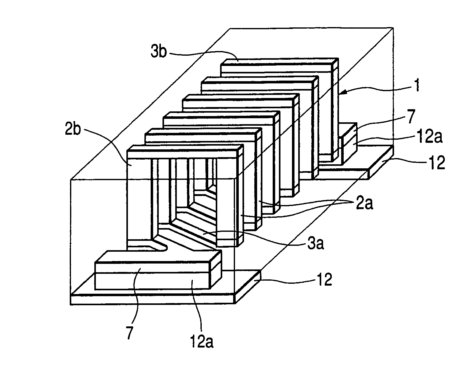
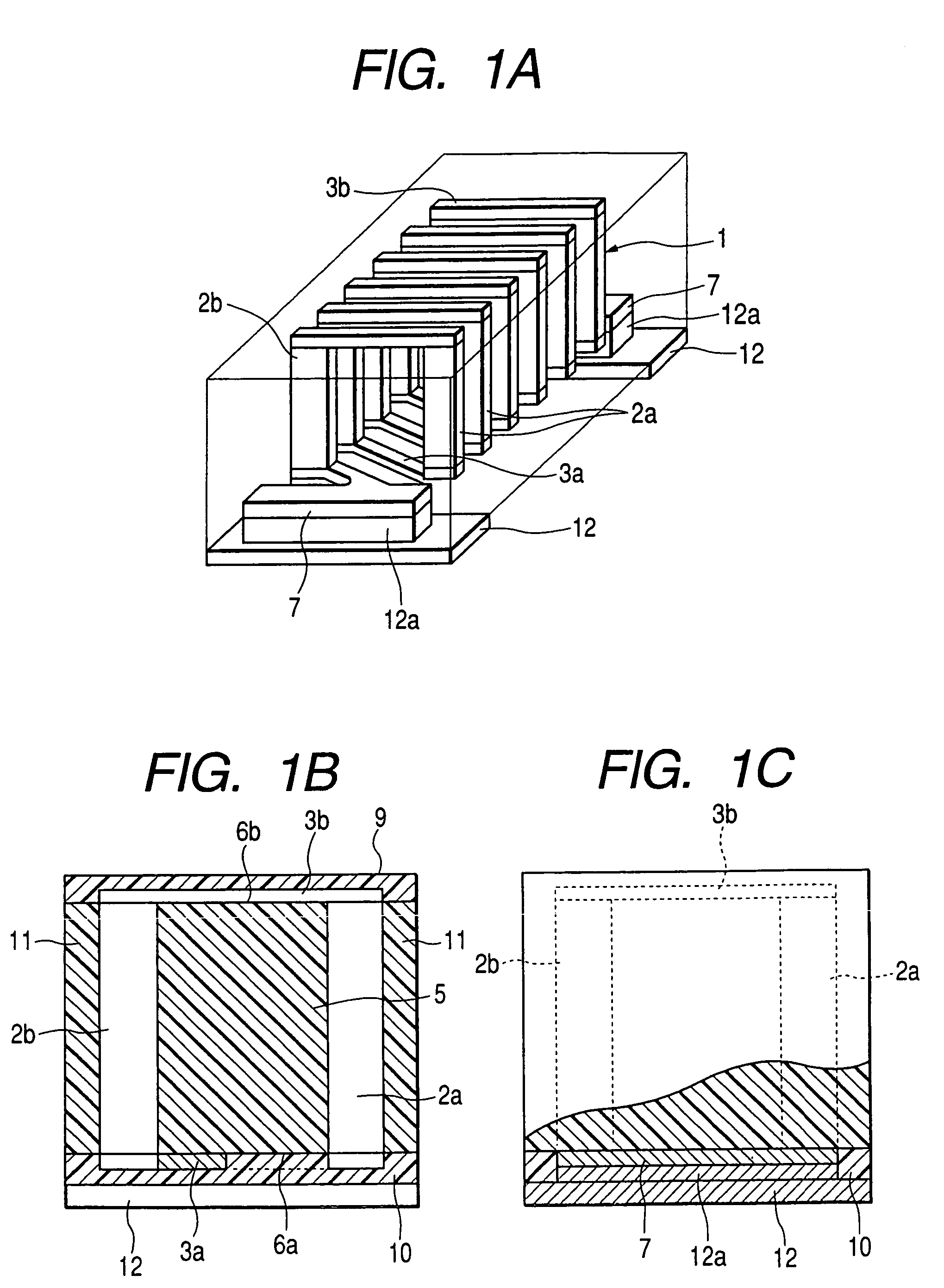
[0087]FIG. 1A is a see-through perspective view showing an embodiment of an inductance element according to the invention.

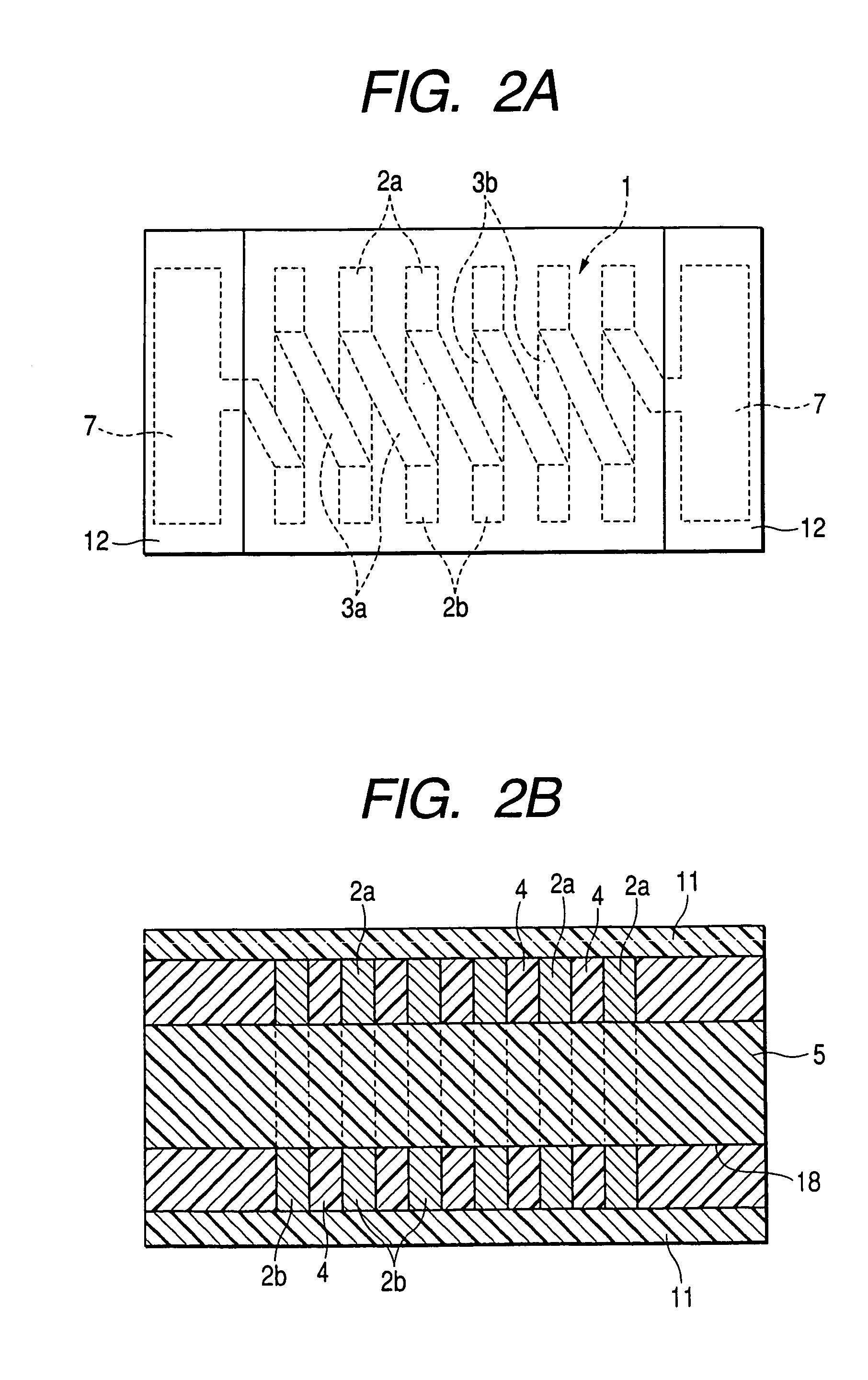
[0088]FIG. 1B is a sectional view showing the configuration of a coil in the inductance element. FIG. 1C is a sectional view showing the structure of an electrode in the inductance element. FIG. 2A is a bottom view of the inductance element. FIG. 2B is a sectional view of the inductance element.

[0089]In FIGS. 1A to 1C and FIGS. 2A and 2B, the reference numeral 1 designates a rectangular helical coil. The coil 1 includes pairs of parallel conductor pieces 2a and 2b, and pairs of bridging conductor pieces 3a and 3b. Each pair of parallel conductor pieces 2a and 2b form two of four sides of one turn of the coil 1. Each pair of bridging conductor pieces 3a and 3b form the other two sides of one turn of the coil 1. Adjacent parallel conductor pieces 2a and 2b are connected to one another by the bridging conductor pieces 3a and 3b respectively to thereby form the recta...


PUM


Abstract

A laminated electronic component including at least one inductance element and produced from a laminate having electrical insulators and electrical conductors laminated alternately. The inductance element is formed as a helical coil having a plurality of turns each constituted by four sides. The inductance element has pairs of parallel conductor pieces and pairs of bridging conductor pieces. Each pair of parallel conductor pieces form two of the four sides of one turn of the coil. Each pair of bridging conductor pieces form the other two sides of one turn of the coil. Grooves are formed in the laminate to thereby form the parallel conductor pieces. The grooves are filled with an electrically insulating material. The bridging conductor pieces are formed on the electrically insulating material.

Description

BACKGROUND OF THE INVENTION[0001]The present invention relates to an inductance element, a laminated electronic component with at least built in inductance and capacitance elements, a laminated electronic component module with at least one built-in inductance element among inductance and capacitance elements, and a method for producing these element, component and module.[0002]For example, Patent Document 1 has disclosed a ceramic electronic component having a laminated inductor and a laminated capacitor integrally piled by a printing method as a laminated electronic component with built-in inductance and capacitance elements.[0003]For example, Patent Document 2 has disclosed a ceramic electronic component having a laminated inductor and a laminated capacitor integrally piled by a sheet laminating method.[0004]For example, Patent Document 3 has disclosed an electronic component having a multi-layer spiral coil formed on a semiconductor chip.[0005]For example, Patent Document 4 has d...

Claims


Application Information

Patent Timeline
IPC IPC(8): H01F5/00H01F17/00H01F17/02H01F27/00H01F41/04H05K1/16H05K3/46
CPCH01F17/0033H01F41/041H05K1/165H05K3/4602H05K2201/097H01L2924/19105H01L2224/48091H01L2224/48227H01L2924/00014B62M3/08
Inventor TAKAYA, MINORUENDO, TOSHIKAZU
Owner TDK CORPARATION
Why Eureka
Try Eureka