Illumination apparatus, projection exposure apparatus, and device fabrication method

a technology of exposure apparatus and illumination apparatus, which is applied in the field of exposure apparatus, can solve the problems of incompatibility with use of refraction elements or lenses, material absorption remarkably increases, and the limit of lithography using ultraviolet light to satisfy the imminent demands for finer semiconductor devices, etc., and achieve the effect of improving throughpu

Inactive Publication Date: 2006-07-25
CANON KK
View PDF20 Cites 9 Cited by
  • Summary
  • Abstract
  • Description
  • Claims
  • Application Information

AI Technical Summary

Problems solved by technology

The lithography using the ultraviolet light has the limit to satisfy the imminent demands for finer semiconductor devices.
As the exposure light has a shorter wavelength, its absorption remarkably increases in a material, and becomes incompatible with use a refraction element or lens for visible light and ultraviolet light.
The energy of most of the absorbed exposure light turns to residual heat and causes temperature rises of mirror and the reticle.
When the temperature rises in mirrors in the projection optical system as a result of exposure light absorptions, a deformed surface shape possibly exceeds the permissible shape error, and makes imaging performance insufficient, i.e., lowered resolution and contrast and insufficient transfers of fine patterns.
This requires, however, an extremely long time for a temperature distribution to turn to a steady state.
In addition, a long standby time to exposure or long non-exposure time would decrease the temperatures of the mirrors and reticle, which have been at the steady state, and the exposure restart delays by several hours or longer for thermal stability.
However, it is difficult for heating means having a wavelength different from that of the exposure light to heat a mirror and reticle like the exposure time, because the mirror and reticle have different absorptive coefficients to optical energy according to light's wavelengths.
Strict coincidence of the temperature rise with that at the exposure time requires one by one heating of a mirror, making the structure complicated and increasing the cost.
However, the standby time that iterates, similar to the exposure time, a procedure that includes the steps of introducing a wafer, fixing the wafer on the wafer chuck, irradiating the exposure light onto the wafer, and taking out the wafer, causes problems, such as arduous wafer carrying in and out, and worn contact parts in a wafer feeding system.
Therefore, when the exposure starts form the standby time, the temperature of the wafer chuck that absorbs the wafer varies, deforms the wafer, and deteriorates the transfer precision.

Method used


Image

  • Illumination apparatus, projection exposure apparatus, and device fabrication method
  • Illumination apparatus, projection exposure apparatus, and device fabrication method
  • Illumination apparatus, projection exposure apparatus, and device fabrication method

Examples


Embodiment Construction

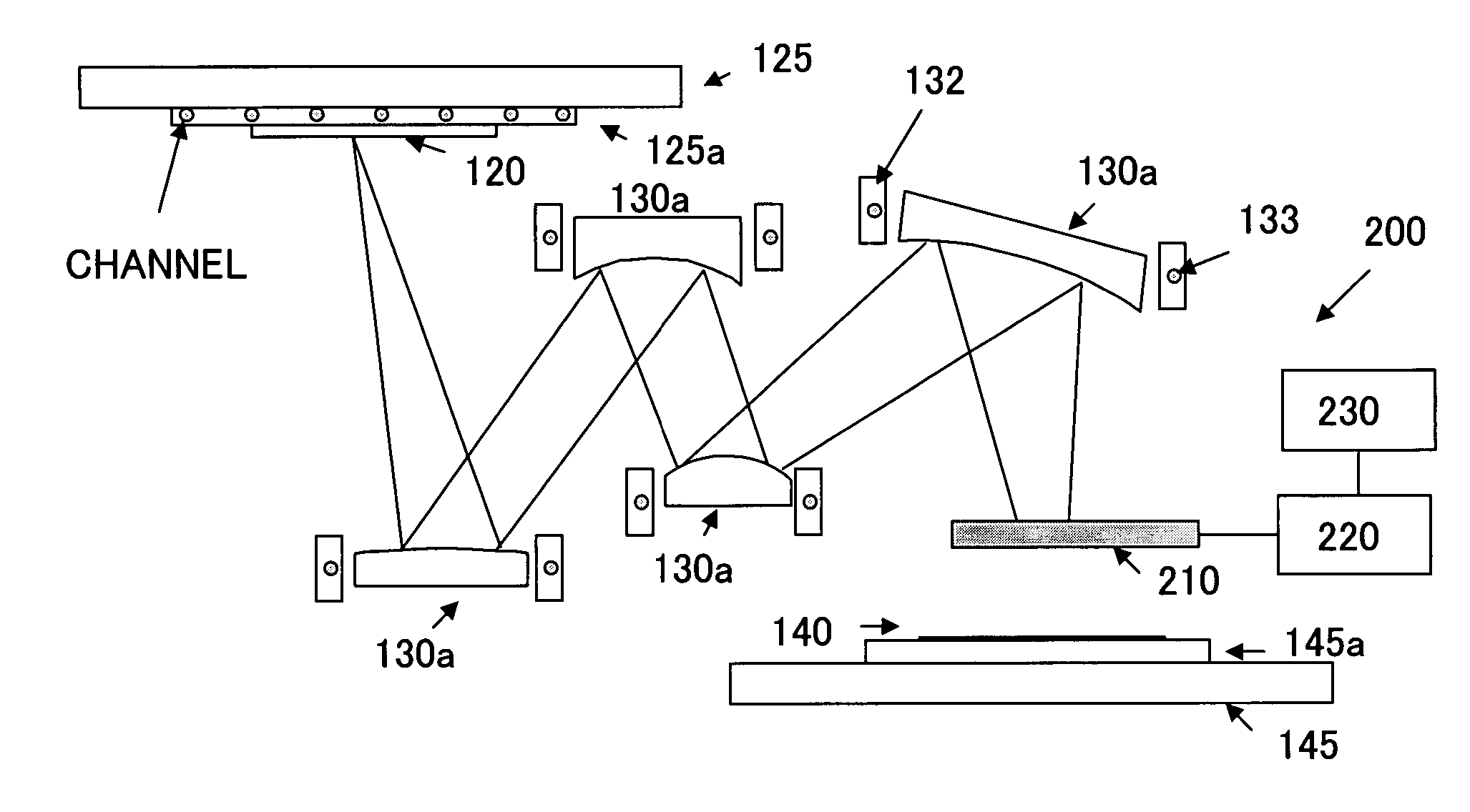
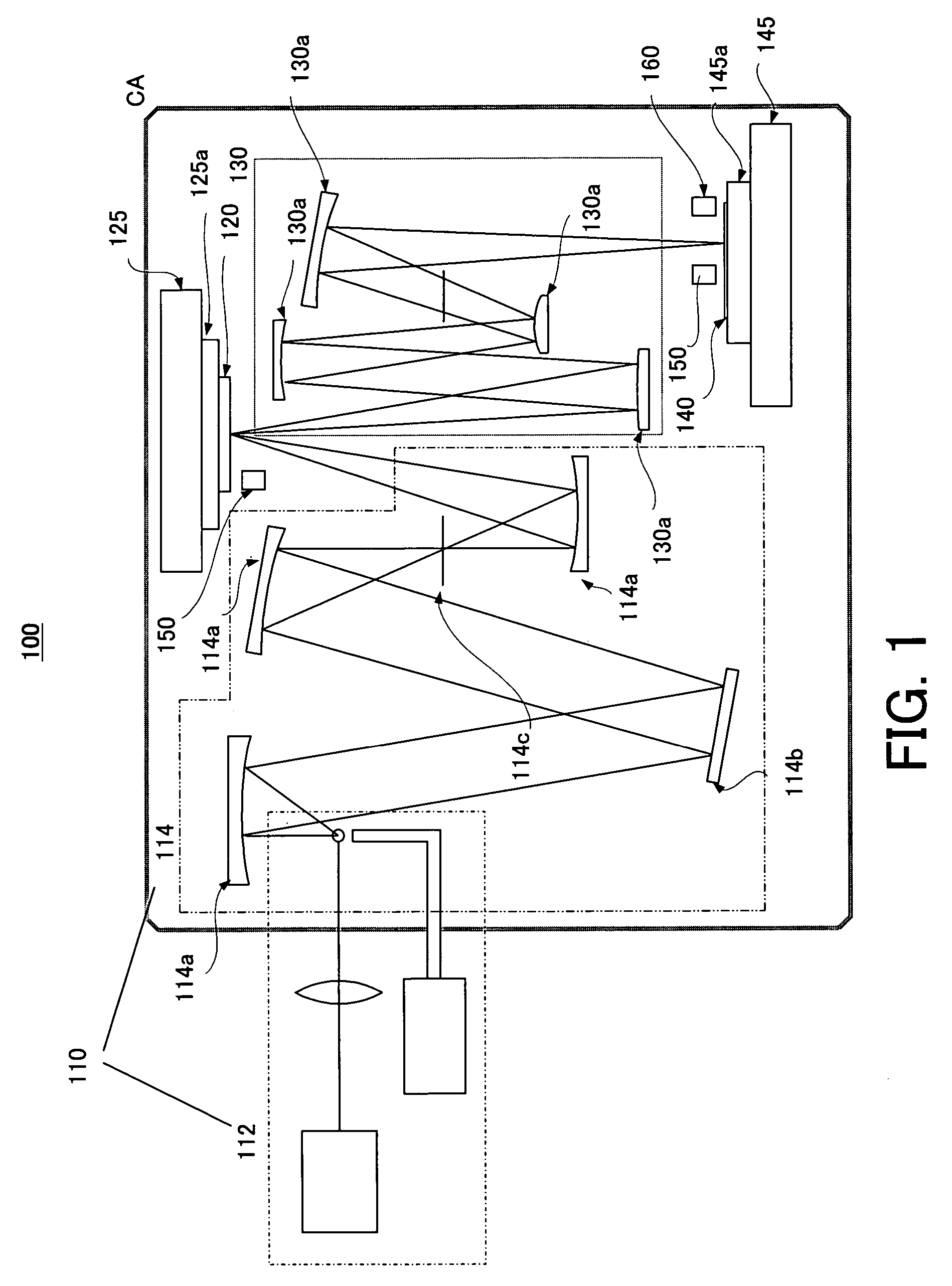
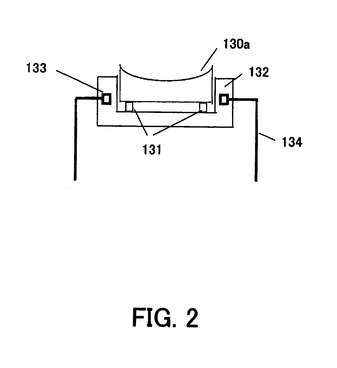
[0035]A detailed description will now be given of an exposure apparatus 100 of one embodiment according to the present invention, with reference to accompanying drawings. In each figure, the same element is designated by the same reference numeral, and a description thereof will be omitted. Here, FIG. 1 is a schematic structure of the exposure apparatus 100.

[0036]The inventive exposure apparatus 100 is a projection exposure apparatus that uses, as illumination light for exposure, EUV light (e.g., with a wavelength of 13.4 nm) to perform a step-and-scan or step-and-repeat exposure that transfers a circuit pattern on a mask 120 onto a substrate 140 to be exposed. Such an exposure apparatus is suitably applicable to a lithography process below submicron or quarter-micron, and a description will be given below of this embodiment exemplarily using a step-and-scan exposure apparatus (which is also called “a scanner”). The step-and-scan manner, as used herein, is an exposure method that ex...


PUM

PropertyMeasurementUnit
wavelengthaaaaaaaaaa

Abstract

An exposure apparatus having an exposure mode that transfers a pattern on a reticle onto an object, and a standby mode that waits for exposure includes an optical system for introducing the exposure light to the object in the exposure mode, and a mechanism for allowing the exposure light to enter the reticle and/or the optical system in the standby mode, and for preventing the exposure light from entering the object in the standby mode.

Description

[0001]This application claims a benefit of foreign priority based on Japanese Patent Application No. 2003-016961, filed on Jan. 27, 2003, which is hereby incorporated by reference herein in its entirety as if fully set forth herein.BACKGROUND OF THE INVENTION[0002]The present invention relates to an exposure apparatus, and more particularly to an exposure apparatus used to manufacture devices, such as a single crystal substrate for a semiconductor wafer and a glass plate for a liquid crystal display (LCD). The present invention is suitable, for example, for an exposure apparatus that uses as exposure light ultraviolet (“UV”) light and extreme ultraviolet (“EUV”) light.[0003]There has conventionally been employed a reduction projection exposure apparatus that uses a projection optical system to project a circuit pattern on a mask (reticle) onto a wafer, etc. to transfer the circuit pattern, in manufacturing such a fine semiconductor device as a semiconductor memory and a logic circui...

Claims


Application Information

Patent Timeline
Patent Type & Authority Patents(United States)
IPC IPC(8): G03B27/72G03B27/42G02B17/06G03F7/20H01L21/027
CPCG02B17/0663G03F7/70216G03F7/7055G03F7/70891G03F7/70708G03F7/70875G03F7/707
Inventor HARA, SHINICHI
Owner CANON KK
Why Eureka
Try Eureka