System and method for correcting timing signals in integrated circuits

a timing signal and integrated circuit technology, applied in the field of timing system for integrated circuits, can solve problems such as existing margins

Inactive Publication Date: 2006-08-01
INT BUSINESS MASCH CORP
View PDF13 Cites 38 Cited by
  • Summary
  • Abstract
  • Description
  • Claims
  • Application Information

AI Technical Summary

Benefits of technology

[0008]It is a further object of the present invention to provide circuitry in IC's for ensuring that data send and receive rates within the IC are maximized in accordance with the physical characteristics and operating conditions of the IC.
[0009]It is another object of the present invention to provide for serial communications transmitters and receivers, a system and methodology for maximizing data send and receive rates within the IC in accordance with the physical characteristics and operating conditions of the IC.
[0013]In a third embodiment, a random number generator is generated with any pseudo-random, linearly distributed algorithm known to skilled artisans (such as XORing the bits with themselves). This unique random number is transmitted throughout a data path of a semiconductor CORE circuit comprising various asynchronous busses or serial data streams. In this embodiment, the random data arrives at a data bus output as a data output signal, and is fed back to a comparator device that compares the data output signal with the original random number. The comparator implements logic for comparing the random data received from the CORE to the random data that was sent into the core. If the data is correct, the output of the comparator circuit will generate signals for enabling the clock frequency provided by clock generator circuit 30 to be increased in a manner so as to achieve a maximum value that avoids a failure point.

Problems solved by technology

However, it is the case that typical process and operating conditions are not worst case resulting in existing margins in most worst case paths.

Method used


Image

  • System and method for correcting timing signals in integrated circuits
  • System and method for correcting timing signals in integrated circuits
  • System and method for correcting timing signals in integrated circuits

Examples


first embodiment

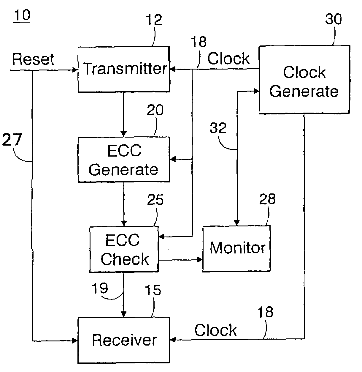
[0020]FIG. 1 is a block diagram depicting the novel error correcting system architecture 10 according to the invention. As shown in FIG. 1, there is provided a source circuit device 12 for transmitting data signals through ECC error correction circuitry 20 to a destination device such as IC receiver device 15 according to clock timing signals 18 provided by clock generator circuit 30. As shown in FIG. 1, the source transmitter circuit 12 is coupled to an error correcting code (ECC) generator circuit device 20 that generates ECC bits in accordance with the data that is received from the transmitter 12. The ECC generator 20 receives data from the transmitter 12 and, outputs the data plus error correction information according to known techniques. Coupled to the ECC generator device 20 is a novel error correcting code (ECC) check circuit device 25 which, in turn, is coupled to a destination receiver device 15 for receiving the transmitted data. As will be described in further detail he...

second embodiment

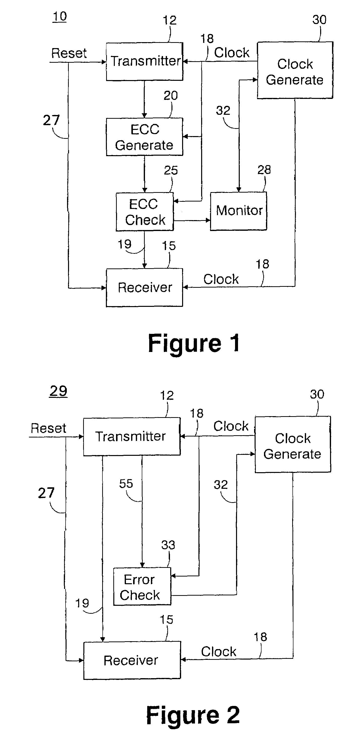
[0023]Preferably, at reset, a learning cycle is implemented where a series of predefined transmissions is generated from the transmit source 12. According to the invention, during the test time, the error check circuitry 33 (FIG. 2) will monitor to a first fail point, and then pick a clock tap of sufficient guard band to guarantee the error free arrival of the data. That is, as the error check circuit 33 is informed of the bit signal patterns output from the transmitter, it knows what signals to expect at each iteration. Thus, during the learning cycle, for each one or a series of outputs generated from the transmit source 12, the clock signal 18 is gradually increased, for example. Thus, the generated signal patterns along line 55 are sufficiently delayed so that they may be read by the error checker circuit 33. As the clock signal 18 input to the transmitter effects the timing of signals generated at the transmit source 12, the error check circuit will monitor the delayed transmi...

third embodiment

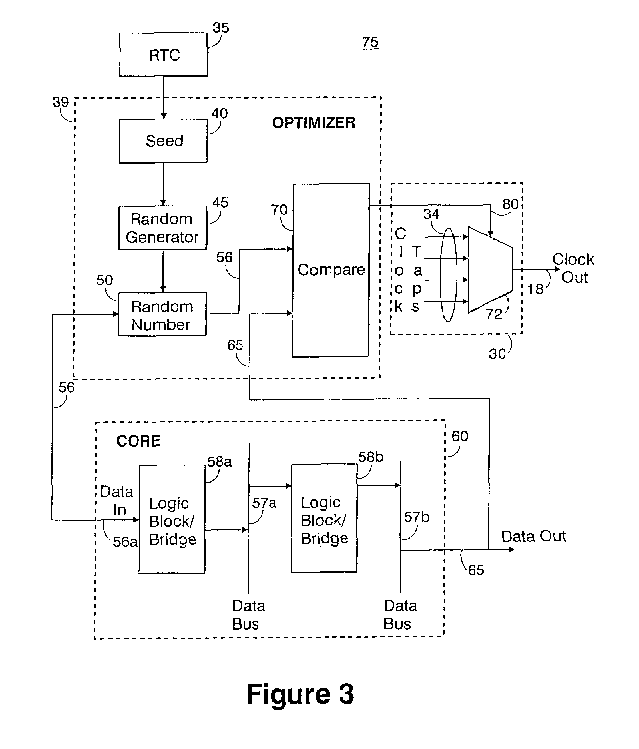
[0027] shown in FIG. 3, there is depicted a detailed dataflow diagram of the error generation and correction circuitry 75. In this embodiment, at system reset, the current value of the Real Time Clock (RTC) 35 is input to an optimizer circuit 39 comprising a SEED register 40 which seeds a random number generator 45. In one embodiment, a SEED is initialized, and then incremented every clock cycle. With this SEED, a unique random number 56 is generated with any pseudo-random, linearly distributed algorithm known to skilled artisans (such as XORing the bits with themselves). This unique random number 56 is transmitted throughout a data path of a semiconductor circuit, e.g., a “system on chip”, also referred to as a CORE circuit 60 comprising the IC, in FIG. 3.

[0028]Particularly, this random data 56 is fed to the start of the dataflow path 56a at the input of the CORE circuit 60 and the data is transmitted through various asynchronous busses or serial data streams. In one embodiment dep...


PUM


Abstract

A system and method for dynamically altering a clock speed of a clock signal used for timing of data signal transmissions and receptions within an integrated circuit (IC) device. The system includes a clock generator circuit for providing a clock signal used for timing of data signal transmission and reception within the IC; a monitoring circuit for receiving data transmissions generated at different clock speeds and detecting when a data transmission fail point is achieved at a particular clock speed; and, a device for adjusting the clock speed according to a maximum speed allowed for the IC that avoids the data transmission fail point.

Description

BACKGROUND OF THE INVENTION[0001]1. Field of the Invention[0002]This invention relates generally to timing systems for integrated circuits (IC's), and more specifically, to novel circuits for altering the clock speed used to send and receive data within the IC based on physical characteristics of the IC.[0003]2. Discussion of the Prior Art[0004]In current integrated circuit design technology, circuits are typically designed to meet the worst case operating condition and technology process conditions. However, it is the case that typical process and operating conditions are not worst case resulting in existing margins in most worst case paths. If the design can take advantage of the real world margin, then significant performance gain could result.[0005]It would thus be highly desirable to provide an Integrated Circuit equipped with error correction circuitry for ensuring that data send and receive rates within the IC are maximized.[0006]It would be further highly desirable to provid...

Claims


Application Information

Patent Timeline
Patent Type & Authority Patents(United States)
IPC IPC(8): G06F11/08G06F11/00H04L1/00
CPCH04L1/0017H04L1/0009
Inventor GOODNOW, KENNETH J.JENKINS, PETER J.KAMPF, FRANCIS A.NORMAN, JASON M.VENTRONE, SEBASTIAN T.
Owner INT BUSINESS MASCH CORP
Why Eureka
Try Eureka