
Chemical-mechanical polishing (CMP) slurry and method of planarizing surfaces

a technology of chemical-mechanical polishing and slurry, which is applied in the direction of manufacturing tools, multi-stage water/sewage treatment, other chemical processes, etc., can solve the problems of poor surface quality, less than desirable polishing rate of polishing slurry, and inconvenient use of slurry

Inactive Publication Date: 2006-08-08
AMCOL INTERNATIONAL CORPORATION
View PDF17 Cites 11 Cited by
  • Summary
  • Abstract
  • Description
  • Claims
  • Application Information

AI Technical Summary

Benefits of technology

"The patent describes a method for polishing semiconductor wafer surfaces using purified clay particles as abrasive particles. The method involves contacting the surface with a composition that includes a liquid carrier, purified clay, and optionally additives such as a chemical accelerator and a complexing or coupling agent. The complexing agent prevents the removed metal and insulator particles from returning to the surface. The method also involves using cation-exchangeable, sodium-free clay particles as the abrasive material. The clay particles are dispersed in a water / clay particle slurry with a particle size range of 0.002 μm to 10 μm. The composition also includes an oxidizing agent accelerator, a chelating agent or complexing agent, and a chelating agent or complexing agent in an amount of 0.1 wt. % to about 20 wt. % of the slurry. The technical effects of the patent include improved surface planarization and reduced defects during semiconductor manufacturing."

Problems solved by technology

Conventional polishing compositions typically are not entirely satisfactory at planarizing semiconductor wafers or integrated circuits having alternating layers of conductive metal and insulating material, e.g., silicon dioxide, that require planar surfaces.
In particular, polishing slurries can have less than desirable polishing rates, and their use in chemically-mechanically polishing semiconductor surfaces can result in poor surface quality.
The difficulty in creating an effective polishing composition for semiconductor wafers stems from the complexity of the semiconductor wafer.
Various problems in semiconductor fabrication can occur if the process steps are not performed on wafer surfaces that are adequately planarized.

Method used


Image

  • Chemical-mechanical polishing (CMP) slurry and method of planarizing surfaces
  • Chemical-mechanical polishing (CMP) slurry and method of planarizing surfaces
  • Chemical-mechanical polishing (CMP) slurry and method of planarizing surfaces

Examples


examples

[0049]The following examples further illustrate the present invention but, of course, should not be construed as in any way limiting its scope.

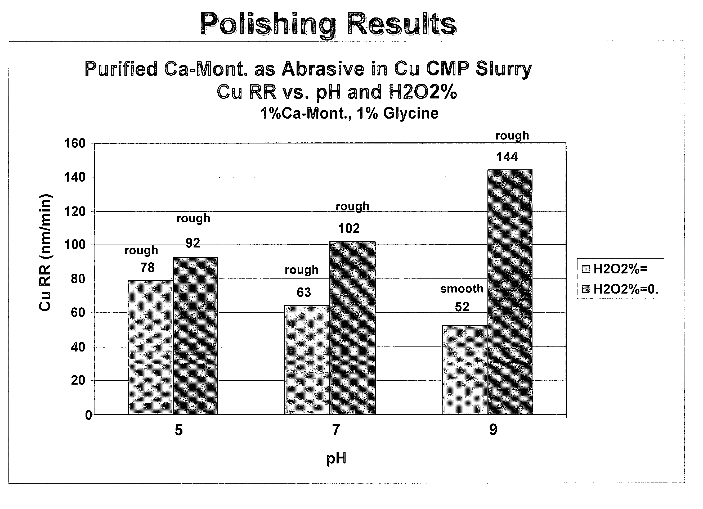
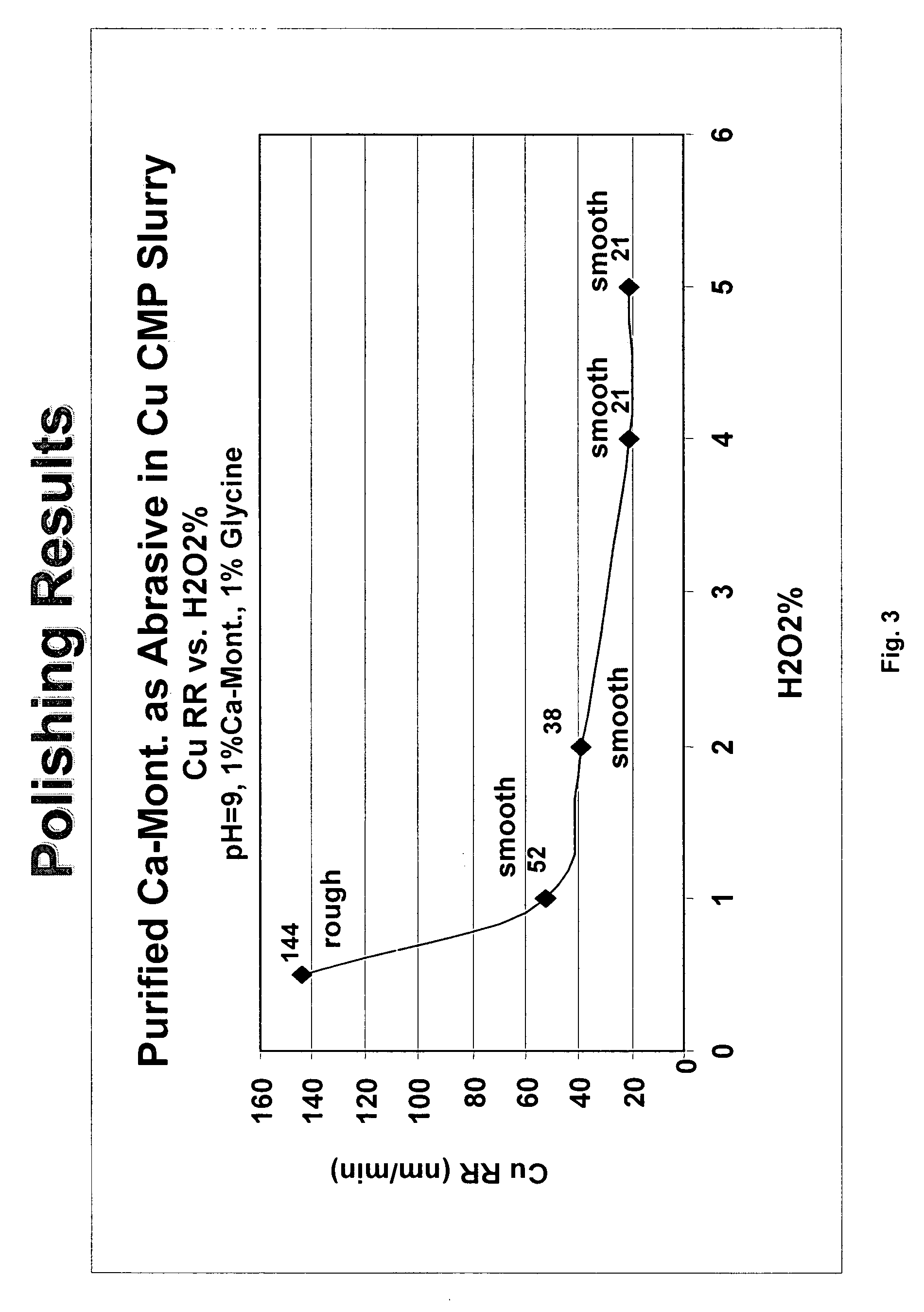
[0050]FIGS. 3 and 4 are graphs showing the rate of copper removal using the slurry polishing compositions of the preferred embodiment (the calcium montmorillonite clay shown in Tables I and II. The polishing experiments were carried out using a bench-top Struers DAP-V polisher having a diameter of 31.75 mm for polishing 99.999% pure copper disks. The polishing pads were IC-1400 provided by Rodel, Inc. The pads were hand-conditioned with 220-grit sandpaper and a nylon brush before being used. The center-to-center distance between the disk and the pad was 5.5 cm. The polishing table and the disk holder are both rotated at a speed of 100 rpm in the same clockwise direction. The applied downward pressure is 5 psi and the slurry flow rate is 30 ml / min. The polishing rates were determined from the mass loss of copper from the disks during 3 min, 6 ...


PUM

PropertyMeasurementUnit
particle sizeaaaaaaaaaa

Abstract

A chemical-mechanical abrasive composition for use in semiconductor processing uses abrasive particles having a non-spherical morphology.

Description

TECHNICAL FIELD[0001]The present invention is directed to a clay-containing abrasive composition and method of planarizing or polishing metal and / or insulator (dielectric) surfaces. The composition is used as purified clay-containing aqueous slurry, particularly useful in the manufacture of semiconductor devices, e.g., integrated circuits, wafers, memory disks and rigid disks.BACKGROUND[0002]Compositions for planarizing or polishing the surface of a substrate are well known in the art. Polishing slurries typically contain an abrasive material in an aqueous solution and are applied to a surface by contacting the surface with a polishing pad saturated with the slurry composition. Typical abrasive materials include silicon dioxide, cerium oxide, aluminum oxide, zirconium oxide, and tin oxide. U.S. Pat. No. 5,527,423, for example, describes a method for chemically-mechanically polishing a metal layer by contacting the surface with a polishing slurry comprising high purity fine metal oxi...

Claims


Application Information

Patent Timeline
Patent Type & Authority Patents(United States)
IPC IPC(8): H01L21/302C09G1/02C09K3/14H01L21/321
CPCC09G1/02H01L21/3212C09K3/1463C09K3/1409
Inventor FANG, MINGMINGIANIRO, MICHAEL R.EISENHOUR, DON D.
Owner AMCOL INTERNATIONAL CORPORATION
Learn More