Semiconductor device, ball grid array connection system, and method of making

Inactive Publication Date: 2006-08-15
ROUND ROCK RES LLC
View PDF19 Cites 5 Cited by
  • Summary
  • Abstract
  • Description
  • Claims
  • Application Information

AI Technical Summary

Benefits of technology

[0016]The film has electrical conductors (for example, conductive traces, via holes and solder balls) for providing communication between the die and an external device. An advantage of the invention is that the package containing the die may have a small footprint and reduced height, if desired.
[0017]The present invention may be employed with a die that has centrally located bond pads. In addition, the invention may be used in perimeter pad devices. Thus, the metal layer may have a smaller surface area than the die. In another embodiment of the invention, the metal layer has peripheral portions that extend laterally outwardly beyond the edges of the die, for example to provide room for additional rows of solder balls and / or to provide increased heat dissipation. In another embodiment of the invention, the metal layer has a recess that receives or contains the die to provide increased stiffness, protection and / or heat dissipation. The present invention is not limited to the preferred embodiments described herein.
[0018]The invention also relates to a tape-based process for producing semiconductor devices. In a preferred embodiment of the invention, a tape structure is formed of electrically insulative tape, a succession of semiconductor dies attached to the tape, and stiff metal grounding layers. The metal layers are located between the dies and the tape. A corresponding succession of ball grid arrays, wires, or other electrical connection systems, may be located on the tape. Thus, according to the invention, semiconductor devices, workpieces and / or electronic components may be formed according to a tape-based process and subsequently separated from each other.
[0019]The invention also includes a multilayer structure as an alternative to the supporting insulative layer. This multilayer structure can comprise a plurality of insulative layers and circuitry layers in electrical connection with the die, the ball grid array, and / or ground layers. Also, within the multilayer structure, additional grounding or power planes can be provided. The multilayer structure provides improved routability in wiring circuitry and easier ground and power wiring. One or more via holes may also be provided to connect the ball grid array to underlying circuitry or conductive planes incorporated within the multilayer structure.

Problems solved by technology

In addition, as the size of ball grid array devices are reduced and the number and complexity of the required electrical interconnections are increased, it becomes increasingly difficult to produce a satisfactory conductive routing pattern on the resin material.

Method used


Image

  • Semiconductor device, ball grid array connection system, and method of making
  • Semiconductor device, ball grid array connection system, and method of making
  • Semiconductor device, ball grid array connection system, and method of making

Examples


Embodiment Construction

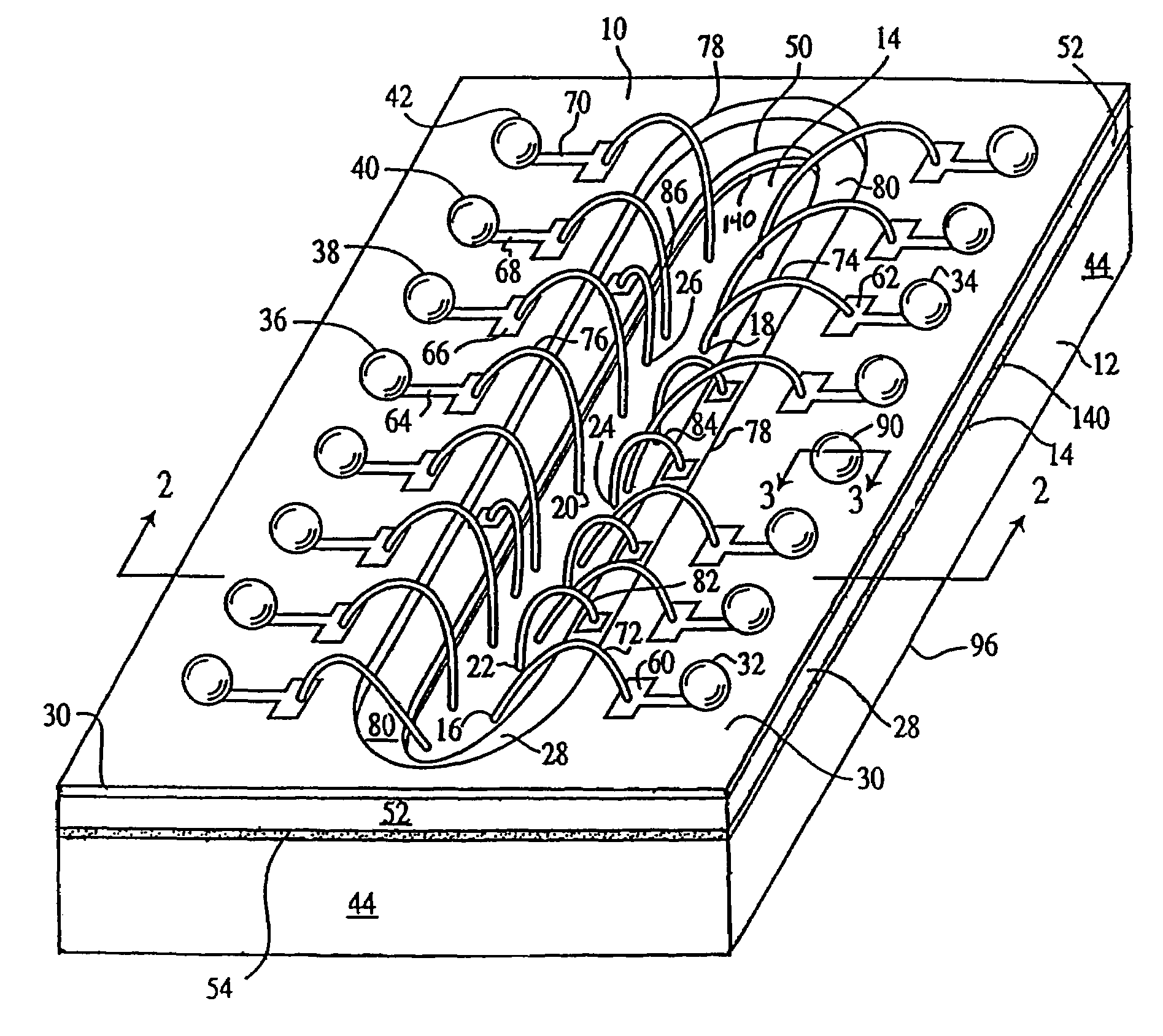
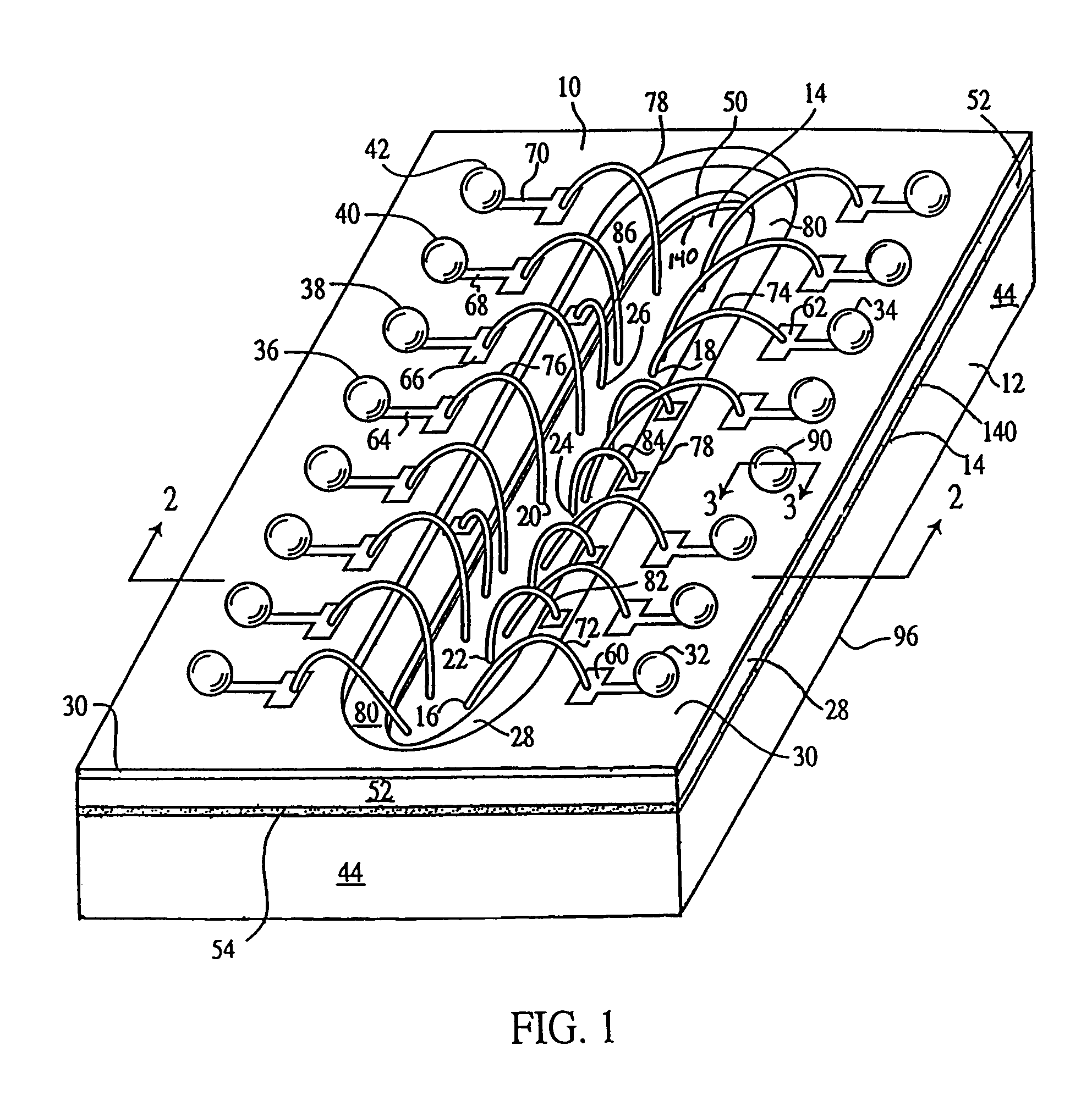
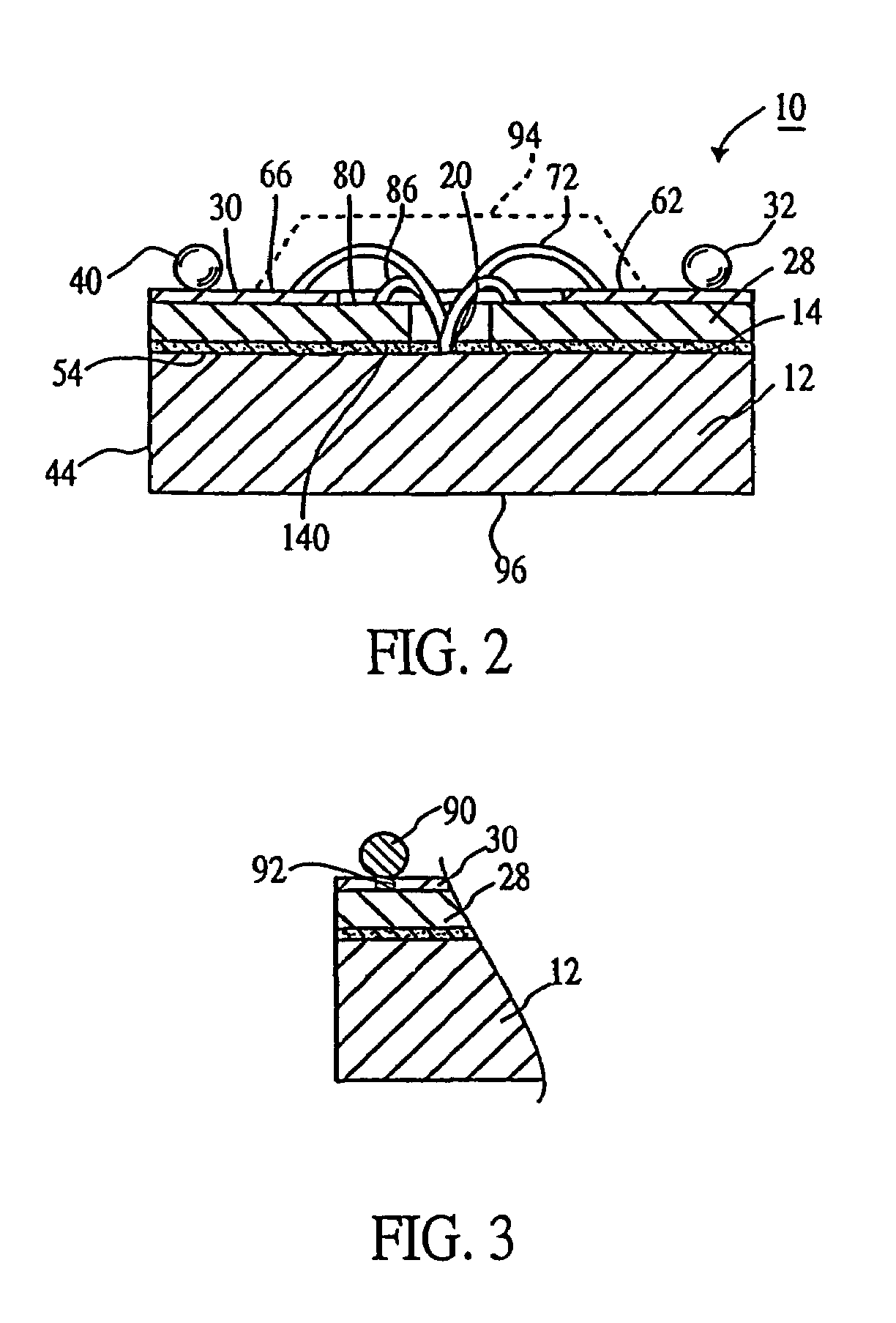
[0031]Referring now to the drawings, where like reference numerals refer to like elements, there is shown in FIG. 1 a board-on-chip (BOC) semiconductor device 10 constructed in accordance with the present invention. The device 10 has a semiconductor die 12 with an active top surface 14. The die 12 contains an integrated circuit (not shown). The integrated circuit is in electrical communication with bond pads 16, 18, 20, 22, 24, 26 on the active surface 14.

[0032]An electrically conductive layer 28 is located on the active surface 14. The conductive layer 28 may be formed of a stiff metal material. An electrically insulative plastic film (or laminate) 30 is located on the metal layer 28. A ball grid array (BGA) is located on the plastic layer 30. The ball grid array is formed of at least two rows of minute solder balls 32, 34, 36, 38, 40, 42. In a preferred embodiment of the invention, the solder balls 32–42 form a fine ball grid array (FBGA). The balls 32–42 may be formed of tin (Sn)...


PUM


Abstract

A semiconductor device is provided with a metal stiffening layer between the die and a multilayer structure comprising at least two insulating layers each having at least one conductor thereon. A top insulating layer of the multilayer structure contains a ball grid array. The metal layer is used as an electrical ground plane to simplify the routing pattern of conductive traces on the insulating material. The metal layer may also be used to dissipate heat from the die. The conductors of the multilayer structure provide additional versatility in wiring the die to the ball grid array.

Description

[0001]This application is a continuation of U.S. patent application Ser. No. 10 / 119,192, now U.S. Pat. No. 6,773,965 filed Apr. 10, 2002; which is a CIP of U.S. application Ser. No. 09 / 653,410, now U.S. Pat. No. 6,372,552 filed Aug. 31, 2000; which is a divisional of U.S. application Ser. No. 09 / 317,957, now U.S. Pat. No. 6,268,650 filed May 25, 1999. The entirety of these applications and patents is hereby incorporated by reference.BACKGROUND OF THE INVENTION[0002]1. Field of the Invention[0003]The present invention relates generally to structures for providing electrical connections and / or interconnections for semiconductor devices. More particularly, the invention relates to ball grid array (BGA) packages, and conductive structures for connecting integrated circuits to ball grid arrays, including fine ball grid arrays (FBGA). The present invention also relates to methods of making electronic devices and the like, particularly tape-based methods of manufacturing semiconductor devi...

Claims


Application Information

Patent Timeline
IPC IPC(8): H01L29/40H01L23/31
CPCH01L23/3107H01L24/97H01L24/48H01L2224/48091H01L2224/4824H01L2224/49109H01L2224/73215H01L2224/97H01L2924/01013H01L2924/01029H01L2924/01082H01L2924/14H01L2924/15311H01L24/49H01L2924/01033H01L2224/32225H01L2924/00014H01L2224/85H01L2224/83H01L2924/00H01L2224/451H01L2924/181H01L24/45H01L2224/05599
Inventor KINSMAN, LARRY D.AKRAM, SALMAN
Owner ROUND ROCK RES LLC
Why Eureka
Try Eureka