Method and apparatus for inspecting a semiconductor wafer

a technology of semiconductor wafers and inspection methods, applied in the direction of instruments, lenses, optical elements, etc., can solve the problems of wafer pattern defects, wafer patterns, presence of contaminant particles and/or scratches on the wafers, etc., and achieve the effect of convenient us

Inactive Publication Date: 2006-08-15
KLA CORP
View PDF9 Cites 66 Cited by
  • Summary
  • Abstract
  • Description
  • Claims
  • Application Information

AI Technical Summary

Benefits of technology

[0013]It is another object of the present invention to provide a method and apparatus as described above which effectively illuminates an area of the semiconductor wafer for detection.
[0015]It is yet another object of the present invention to provide a method and apparatus as described above which includes a dynamic, real-time auto-focusing system for ensuring that the main imaging lens images the illuminated area of the semiconductor wafer onto the main imaging camera in focus.
[0016]It is still another object of the present invention to provide a method and apparatus as described above which has a limited number of parts and which is easy to use.

Problems solved by technology

The most prevalent type of wafer pattern defect which occurs during the manufacturing of patterned semiconductor wafers is the improper deposition of conductive and / or insulated material onto the silicon wafer during the layering process.
Additional types of wafer pattern defects include, inter alia, the presence of contaminant particles and / or scratches on the wafer during the manufacturing process.
As can be appreciated, the presence of a single defect larger than half the width of a conductive line on the silicon wafer can result in the complete failure of a semiconductor chip which is produced from the wafer.
Such a chip has to be discarded which thereby decreases the percentage yield per wafer and increases the overall cost of the individual wafers.
Although well known and widely used in commerce to detect the presence of defects, conventional wafer inspection systems may suffer from a notable drawback.
Because vertical deviations in wafer topology are considerably greater than the depth of field of conventional wafer inspection systems, particular regions on a wafer scanned by a conventional wafer inspection system are often examined out of focus, which is highly undesirable.

Method used


Image

  • Method and apparatus for inspecting a semiconductor wafer
  • Method and apparatus for inspecting a semiconductor wafer
  • Method and apparatus for inspecting a semiconductor wafer

Examples


Embodiment Construction

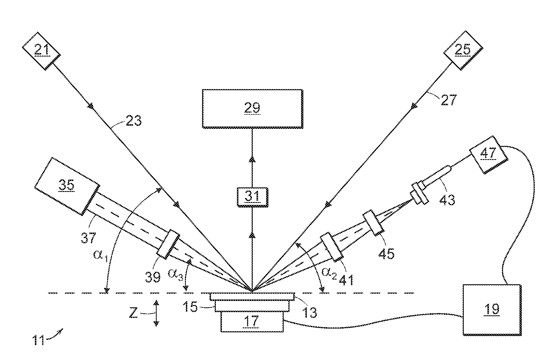
[0023]Referring now to FIG. 1, there is shown a schematic side view representation of an apparatus for inspecting a semiconductor wafer for defects. The apparatus is constructed according to the teachings of the present invention and is identified generally by reference numeral 11.

[0024]Apparatus 11 is shown inspecting a semiconductor wafer 13. Wafer 13 represents any well-known type of semiconductor wafer, such as a patterned semiconductor wafer.

[0025]Semiconductor wafer 13 is retained on a chuck plate 15. Chuck plate 15 is preferably a vacuum chuck plate which is capable of providing a vacuum force for retaining semiconductor wafer 13 securely thereon. Chuck plate 15 is mounted on a stage 17 which is capable of displacing chuck plate 15 in three dimensions (i.e., stage 17 is an X-Y-Z stage), stage 17 being electrically connected to a computer 19. Preferably, stage 17 is a linear motor air-bearing X-Y motion platform which utilizes piezoelectric elements to move chuck plate 15 in t...


PUM

PropertyMeasurementUnit
diameteraaaaaaaaaa
diameteraaaaaaaaaa
diameteraaaaaaaaaa

Abstract

An apparatus for inspecting a semiconductor wafer includes a vertically movable chuck plate for holding said semiconductor wafer, a first light source for illuminating an area on the wafer, a main imaging camera for detecting light scattered from the surface of the wafer and a main imaging lens for imaging the illuminated area of the wafer onto the camera. The apparatus additionally includes an auto-focus system for maintaining the wafer within the depth of field of the lens focal point. The auto-focus system comprises a second light source with associated optics, a linear position sensor with associated optics for detecting light from the second light source that is reflected off the illuminated area of the wafer, circuitry for converting the light detected by the sensor into an output voltage which is proportional to the relative vertical position of the illuminated area of the wafer. In use, the output voltage can be used to compensate for vertical deviations in the topology of said patterned wafer by vertically moving the chuck plate in real-time so that the lens images the area on the wafer onto the camera in focus.

Description

BACKGROUND OF THE INVENTION[0001]The present invention relates generally to a novel method and apparatus for inspecting a semiconductor wafer for defects.[0002]Integrated circuits (ICs) are commonly manufactured through a series of processing steps. Very often more than a hundred processing steps are performed to produce a properly functioning integrated circuit chip.[0003]A semiconductor material, commonly in the shape of a wafer, serves as the substrate for integrated circuits. Semiconductor ICs are typically manufactured as an assembly of a hundred or more chips on a single semiconductor wafer which is then cut up to produce the individual IC chips. Typically, a wafer made of silicon is used as the integrated circuit substrate, the silicon wafer being approximately 150–300 mm in diameter and 0.6–1 mm thick. During the manufacturing process, the silicon wafer is first polished and cleaned to remove all contaminant particles situated thereon. The silicon wafer is then treated in pr...

Claims


Application Information

Patent Timeline
Patent Type & Authority Patents(United States)
IPC IPC(8): G01N21/88G01V8/00
CPCG01N21/9501
Inventor DARDZINSKI, VICTOR C.
Owner KLA CORP
Why Eureka
Try Eureka