
Phase-frequency detector with linear phase error gain near and during phase-lock in delta sigma phase-locked loop

a phase-locked loop and phase-frequency detector technology, applied in oscillator comparator circuits, angle demodulation by phase difference detection, pulse automatic control, etc., can solve the problem of introducing frequency jitter in the output of the host pll, mismatching of charge pump currents, and virtually impossible matching of such small currents

Active Publication Date: 2006-08-15
NAT SEMICON CORP
View PDF7 Cites 33 Cited by
  • Summary
  • Abstract
  • Description
  • Claims
  • Application Information

AI Technical Summary

Benefits of technology

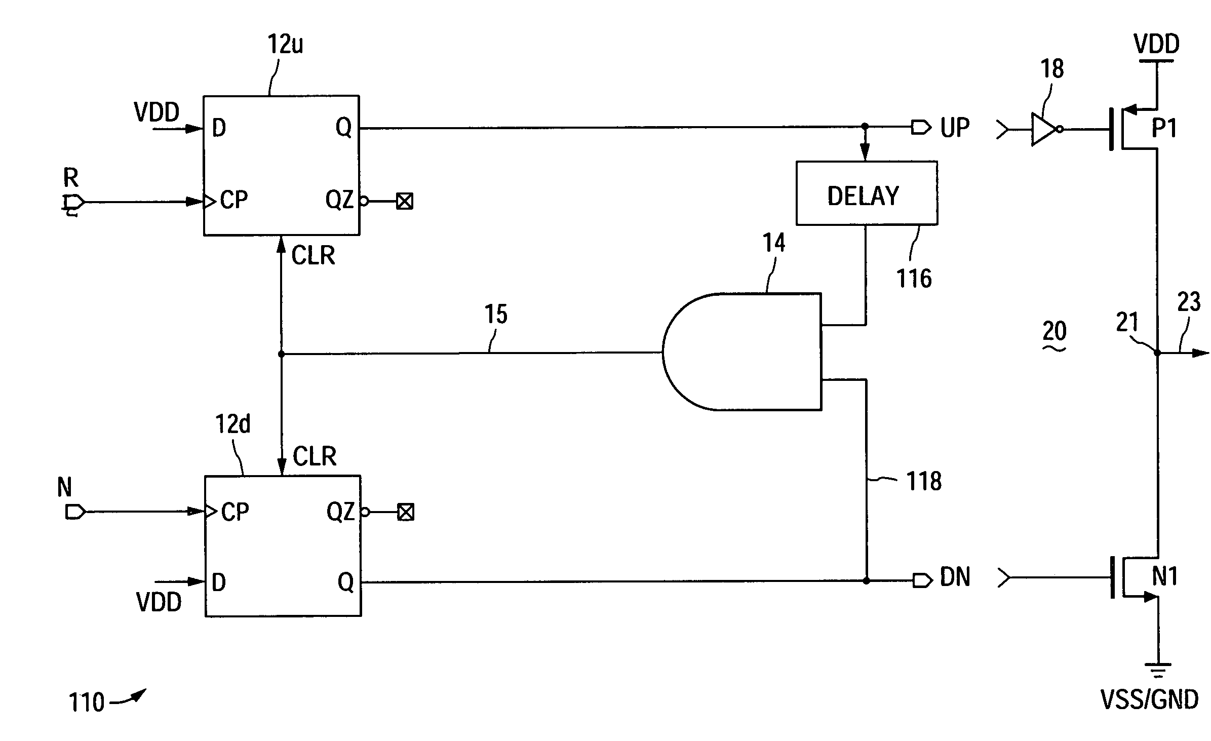
[0012]In accordance with the presently claimed invention, a phase-frequency detector (PFD) is provided with substantially linear phase error gain within a predetermined phase error range centered about zero phase error when used in a delta sigma phase-locked loop (PLL). The output signals (e.g., charge pump control signals), which are also used to reset the input circuitry, are fed back with asymmetrical signal delays, thereby causing one of the output signals to remain in an asserted state for a substantially constant time duration at least during when a difference between the reference and feedback signal phases is within a predetermined phase difference range centered about zero phase difference.

Problems solved by technology

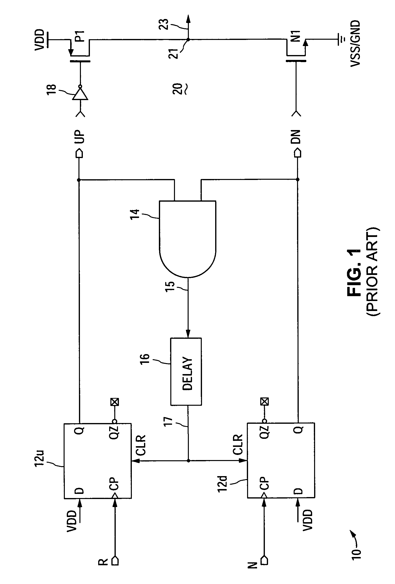
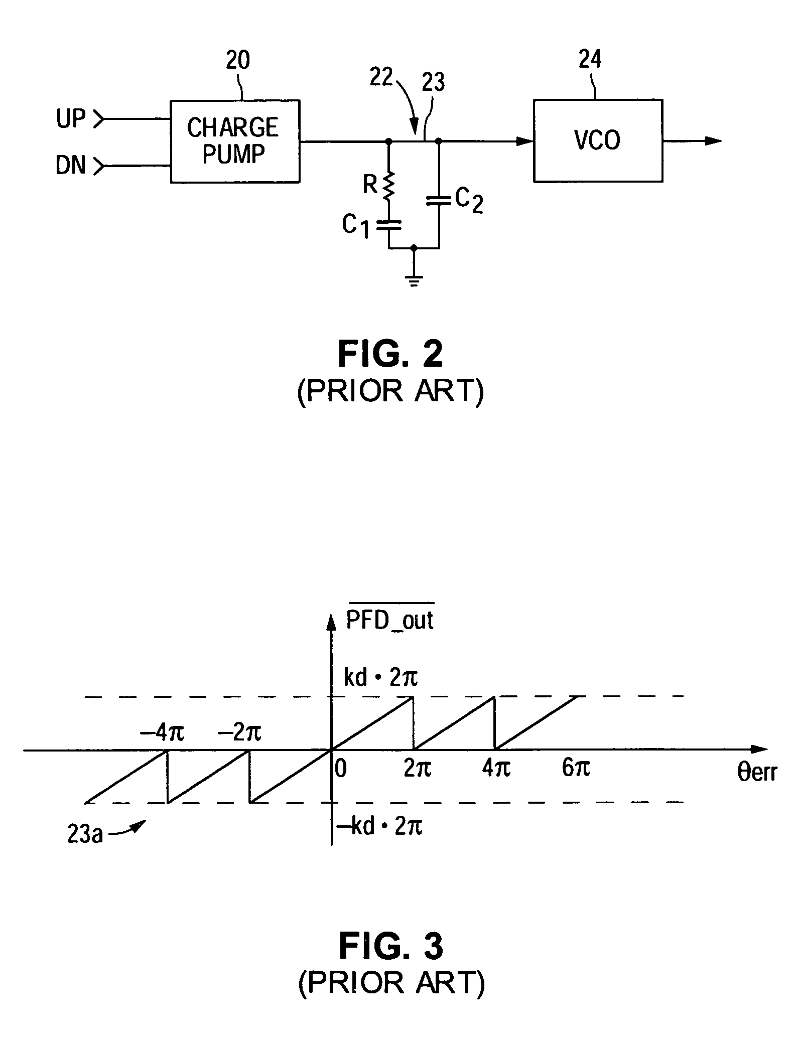
As is well known in the art, phase detectors and PFDs are susceptible to crossover distortion (often referred to as a “dead zone”) within the region D of near-zero phase difference between the two input signals R, N. In this region D, the small signal gain is near zero and can have dramatic changes for very small input phase errors, thereby introducing frequency jitter in the output of the host PLL.
Mismatch between the charge pump currents (pump up and pump down) is a particularly significant problem for delta sigma PLLs due to problems associated with maintaining matched pump up and pump down currents provided by the charge pump 20 to the output terminal 21 (FIG. 1).
Particularly with such currents typically being quite small, and with ever decreasing transistor dimensions, matching such small currents is virtually impossible, particularly over variations in operating conditions (e.g., power supply voltages and circuit operating temperature) and fabrication processes.
As is well known, charge pump current mismatch is a significant problem for delta sigma PLLs because they intentionally introduce large phase errors (positive or negative) to the phase detectors (i.e., multiple VCO pulse periods of error), and it is important that the loop gain remain linear to avoid mixing the high energy, high frequency spurious offset signals down to lower frequencies where the loop filter can no longer adequately suppress them.

Method used


Image

  • Phase-frequency detector with linear phase error gain near and during phase-lock in delta sigma phase-locked loop
  • Phase-frequency detector with linear phase error gain near and during phase-lock in delta sigma phase-locked loop
  • Phase-frequency detector with linear phase error gain near and during phase-lock in delta sigma phase-locked loop

Examples


Embodiment Construction

[0025]The following detailed description is of example embodiments of the presently claimed invention with references to the accompanying drawings. Such description is intended to be illustrative and not limiting with respect to the scope of the present invention. Such embodiments are described in sufficient detail to enable one of ordinary skill in the art to practice the subject invention, and it will be understood that other embodiments may be practiced with some variations without departing from the spirit or scope of the subject invention.

[0026]Throughout the present disclosure, absent a clear indication to the contrary from the context, it will be understood that individual circuit elements as described may be singular or plural in number. For example, the terms “circuit” and “circuitry” may include either a single component or a plurality of components, which are either active and / or passive and are connected or otherwise coupled together to provide the described function. Ad...


PUM


Abstract

A phase-frequency detector (PFD) having substantially linear phase error gain within a predetermined phase error range centered about zero phase error when used in a delta sigma phase-locked loop (PLL). The output signals (e.g., charge pump control signals), which are also used to reset the input circuitry, are fed back with asymmetrical signal delays, thereby causing one of the output signals to remain in an asserted state for a substantially constant time duration at least during when a difference between the reference and feedback signal phases is within a predetermined phase difference range centered about zero phase difference.

Description

BACKGROUND OF THE INVENTION[0001]1. Field of Invention[0002]The present invention relates to digital phase-locked loops (PLLs), and in particular, to phase-frequency detectors (PFD) used in delta sigma PLLs.[0003]2. Description of the Related Art[0004]Referring to FIG. 1, a conventional PFD 10 that has been used in many digital PLL designs (including delta sigma PLLs) includes two D-type flip-flops 12u, 12d, an AND gate 14 and a delay circuit 16, all interconnected substantially as shown. The flip-flops 12u, 12d are separately clocked by the reference signal R and feedback divisor signal N. With each rising edge of these input signals R, N, a logic one (VDD applied at the D-inputs) is clocked through to the output Q of each flip-flop 12U, 12D. The data output signals Q of the flip-flops 12U, 12D form the “pump up” UP and “pump down” DN signals used for controlling a charge pump circuit 20 in accordance with well known principles.[0005]Whenever the reference signal R is asserted, the...

Claims


Application Information

Patent Timeline
Patent Type & Authority Patents(United States)
IPC IPC(8): H03D3/24
CPCH03L7/0891H03D13/004
Inventor HUARD, JEFFREY MARK
Owner NAT SEMICON CORP
Learn More