Semiconductor wafer carrier mapping sensor

Active Publication Date: 2006-08-22
CYBEROPTICS SEMICON
View PDF27 Cites 3 Cited by
  • Summary
  • Abstract
  • Description
  • Claims
  • Application Information

AI Technical Summary

Problems solved by technology

“Cross slots” are wafer position errors where the wafer is not maintained in a single “slot” but erroneously spans a pair of slots.
In this situation, it is important that the tool not attempt to interact with the wafer, but instead generate an error.
Wafer carrier mapping systems have begun to face a difficult challenge recently with the increasing use of dark wafers typically with nitride coatings.
While mapping systems can be adjusted to optimally detect the traditionally light wafers, such as copper or aluminum coated silicon wafers, or the dark nitride wafers, sensing systems do not adequately deal with mixes of

Method used


Image

  • Semiconductor wafer carrier mapping sensor
  • Semiconductor wafer carrier mapping sensor
  • Semiconductor wafer carrier mapping sensor

Examples


Embodiment Construction

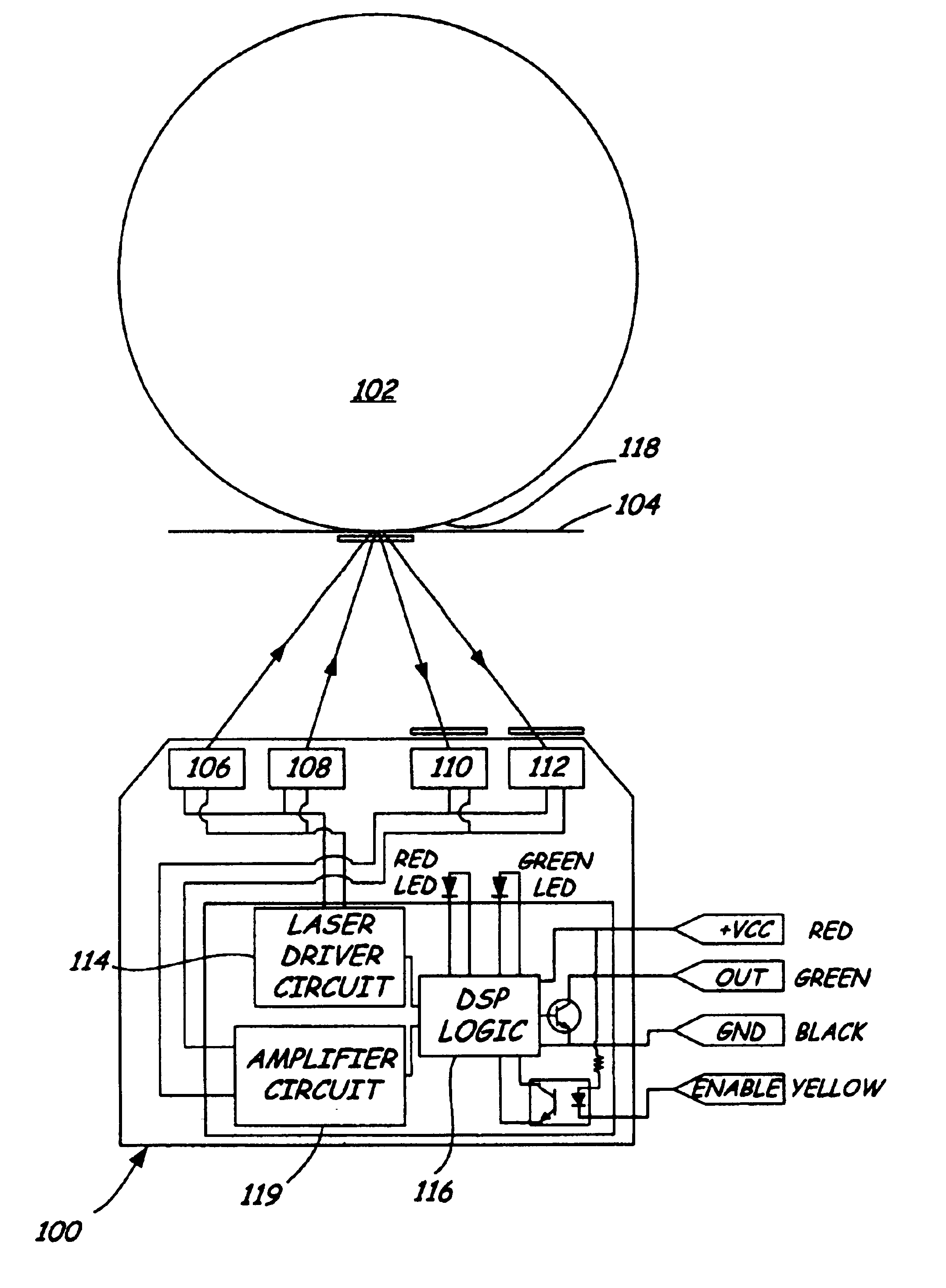
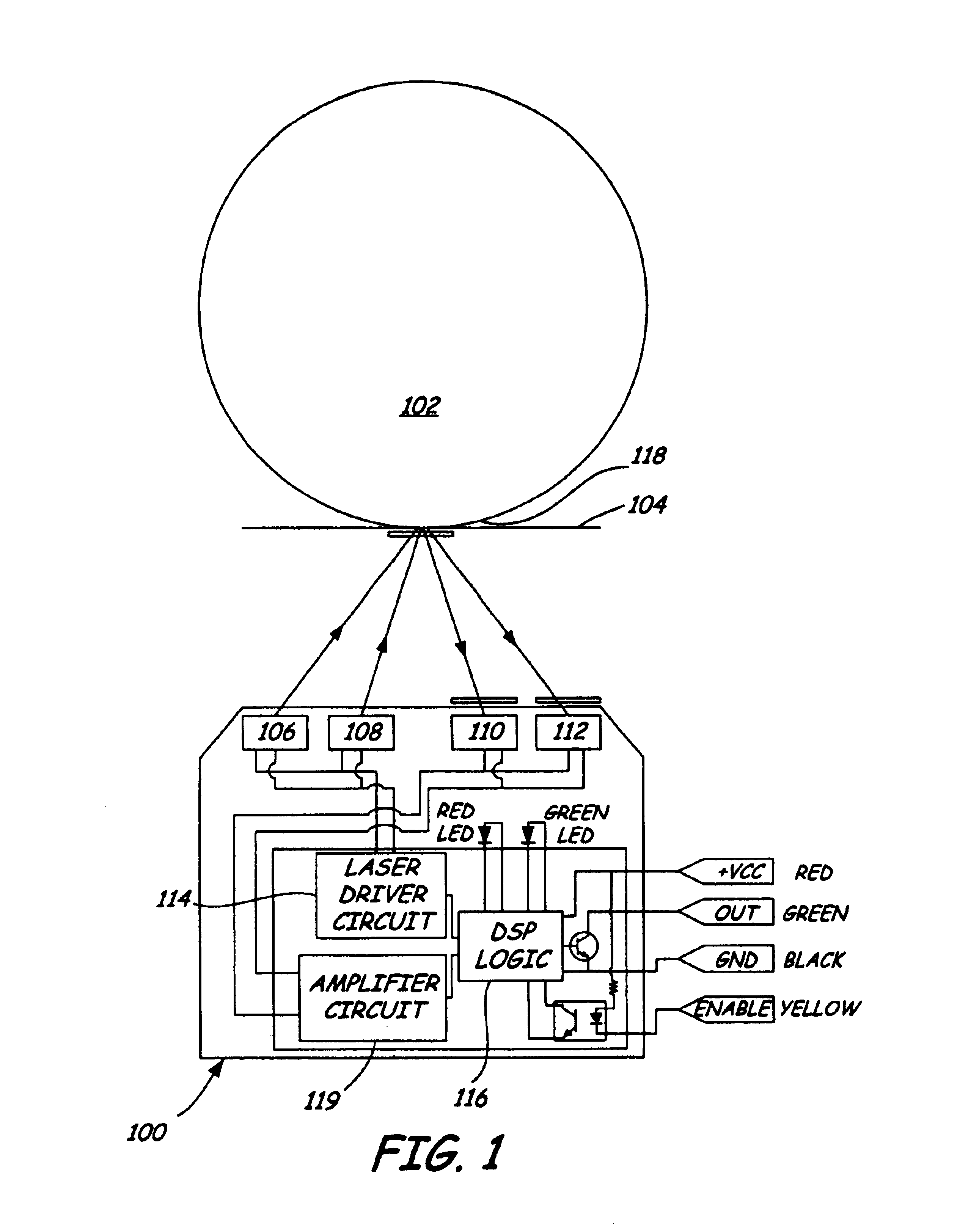
[0012]Embodiments of the present invention are directed to increasing the effective dynamic range of laser-based wafer carrier mapping sensors. Various features and combinations thereof have been explored that synergistically provide significantly advanced wafer detection. These features will be set forth below individually, but it is expressly contemplated that embodiments of the invention are not limited to the individual features but also include the vast array of combinations thereof.

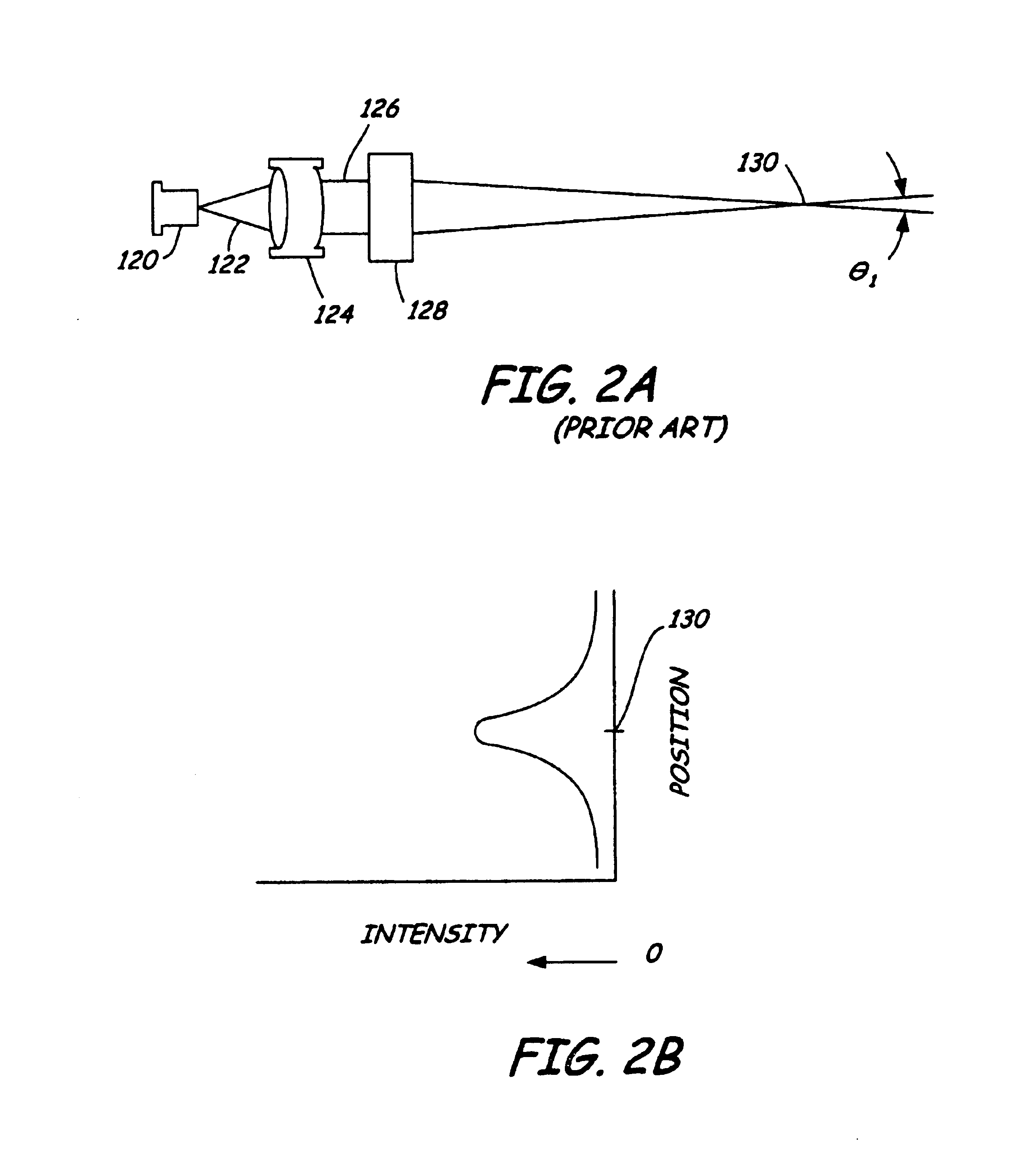
[0013]FIG. 1 is a diagrammatic view of a wafer carrier mapping system in accordance with embodiments of the present invention. FIG. 2 shows a sensor geometry that is more optimum for on-axis applications. Sensor 100 is arranged to detect wafers such as wafer 102 in carrier 104. One example of carrier 104 is a Front Opening Unified Pod (FOUP) Two laser sources, preferably laser diodes, 106 and 108 shine respectively into detectors 110 and 112, when reflected from wafer edge 118. Each of sources 106, ...


PUM


Abstract

An improved laser-based wafer carrier mapping sensor is provided. The sensor includes a number of improvements including laser source improvements; optical improvements; and detector improvements. Laser source improvements include the type of laser sources used as well as the specification of size and power of such sources. Optical improvements include features that intentionally defocus the laser stripe on the wafer as well as additional features that help ensure precision stripe generation. Detector improvements include increasing gain while decreasing the effects of ambient light. Various combinations of these features provide additional synergies that facilitate the construction of a sensor with significantly improved dynamic response while decreasing the frequency of false cross slot errors.

Description

CROSS-REFERENCE OF CO-PENDING APPLICATIONS[0001]The present application claims priority to previously filed co-pending provisional application Ser. No. 60 / 341,494, filed Dec. 17, 2001, entitled IMPROVED MAPPING SENSOR, which application is incorporated herein by reference in its entirety.BACKGROUND OF THE INVENTION[0002]Wafer carrier mapping sensors are used in the manufacture and processing of semiconductor wafers to detect wafers in a wafer carrier. In order to effectively process the wafers in the carrier, the semiconductor tool must know which positions within the carrier have wafers, and whether those wafers are properly held therein. Wafer carrier mapping sensors scan the wafer edges to detect wafer absence / presence and additionally errors such as cross slots. “Cross slots” are wafer position errors where the wafer is not maintained in a single “slot” but erroneously spans a pair of slots. In this situation, it is important that the tool not attempt to interact with the wafer,...

Claims


Application Information

Patent Timeline
IPC IPC(8): H01S3/13G01B11/00H01L21/00H01L21/67H01L21/673
CPCH01L21/67265H01L21/6735H01L21/68
Inventor SCHUDA, FELIX J.
Owner CYBEROPTICS SEMICON
Why Eureka
Try Eureka