Vertical cavity surface emitting laser including indium, antimony and nitrogen in the active region

a laser and active region technology, applied in lasers, semiconductor lasers, nanotechnology, etc., can solve the problems of strain in quantum wells, inability to test edge emitting lasers, and difficult efficient collection of emitted beams, so as to achieve excellent carrier confinement and reduce the thickness of quantum wells

Inactive Publication Date: 2006-08-22
II VI DELAWARE INC
View PDF118 Cites 30 Cited by
  • Summary
  • Abstract
  • Description
  • Claims
  • Application Information

AI Technical Summary

Benefits of technology

[0022]In accordance with another aspect of the present invention, Nitrogen can be added to the barrier layers of the InGaAs quantum wells of a VCSEL such that the barrier layers are in tension while the quantum wells are in compression. To compensate for the property changes inherent with the addition of Nitrogen to InGaAs quantum wells, quantum well thickness can be reduced. Nitrogen can be useful for strain compensation and overall band gap reduction within the active region.
[0023]In accordance with another feature of the present invention, AlGaAs or AlGaAsN can be used for minority carrier confinement in the barrier layers to avoid type 2 behavior in the valence band.
[0024]In accordance with another feature of the present invention, Nitrogen or nitrogen and Sb can be used in GaAs or InGaAs quantum wells. The Sb and nitrogen are balanced to avoid a type 2 transition in either the valence band or the conduction band and maintain excellent carrier confinement with at least a 0.1 ev band discontinuity of both the valence and conduction bands at the quantum well edge.

Problems solved by technology

A reason for the interest in VCSELs is that edge emitting lasers produce a beam with a large angular divergence, making efficient collection of the emitted beam more difficult.
Furthermore, edge emitting lasers cannot be tested until the wafer is cleaved into individual devices, the edges of which form the mirror facets of each device.
In addition, since VCSELs incorporate the mirrors monolithically in their design, they allow for on-wafer testing and the fabrication of one-dimensional or two-dimensional laser arrays.
The use of InGaAs quantum wells, however, causes strain in the quantum wells.
If the quantum wells are grown past their critical thickness, they relax by creating dislocations, and thus a poor quality active region.
Sometimes the confining layers and barrier layers are made from the same compositions, but this is not optimal for carrier confinement and is usually a compromise made for processing reasons.

Method used


Image

  • Vertical cavity surface emitting laser including indium, antimony and nitrogen in the active region
  • Vertical cavity surface emitting laser including indium, antimony and nitrogen in the active region
  • Vertical cavity surface emitting laser including indium, antimony and nitrogen in the active region

Examples


Embodiment Construction

[0050]The novel features of the present invention will become apparent to those of skill in the art upon examination of the following detailed description of the invention or can be learned by practice of the present invention. It should be understood, however, that the detailed description of the invention and the specific examples presented, while indicating certain embodiments of the present invention, are provided for illustration purposes only because various changes and modifications within the scope of the invention will become apparent to those of skill in the art from the detailed description of the invention and claims that follow.

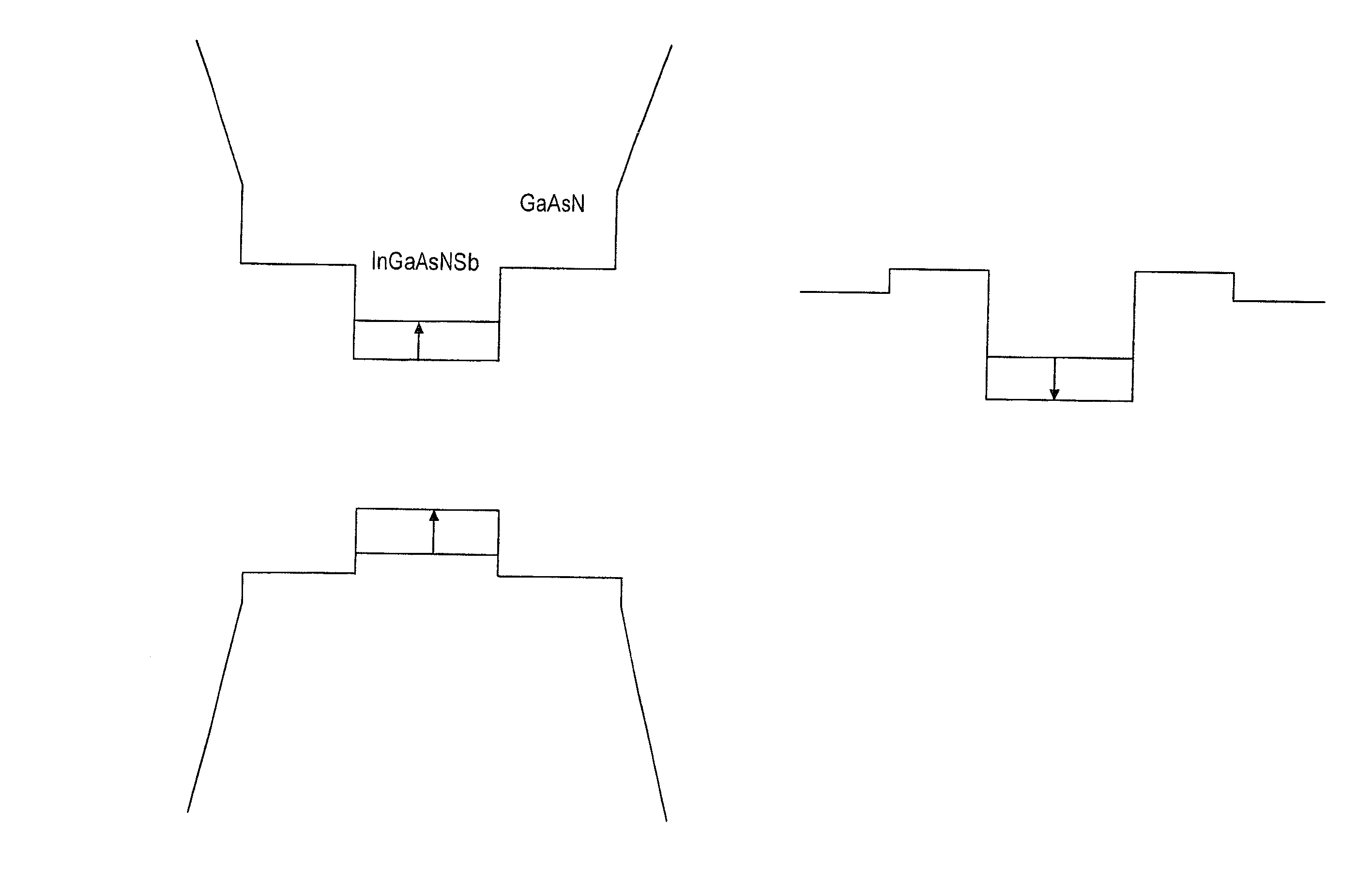
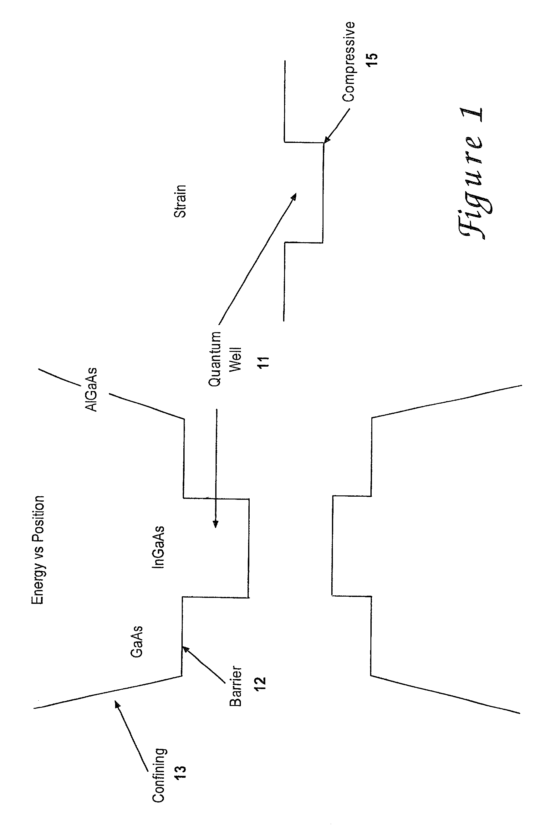
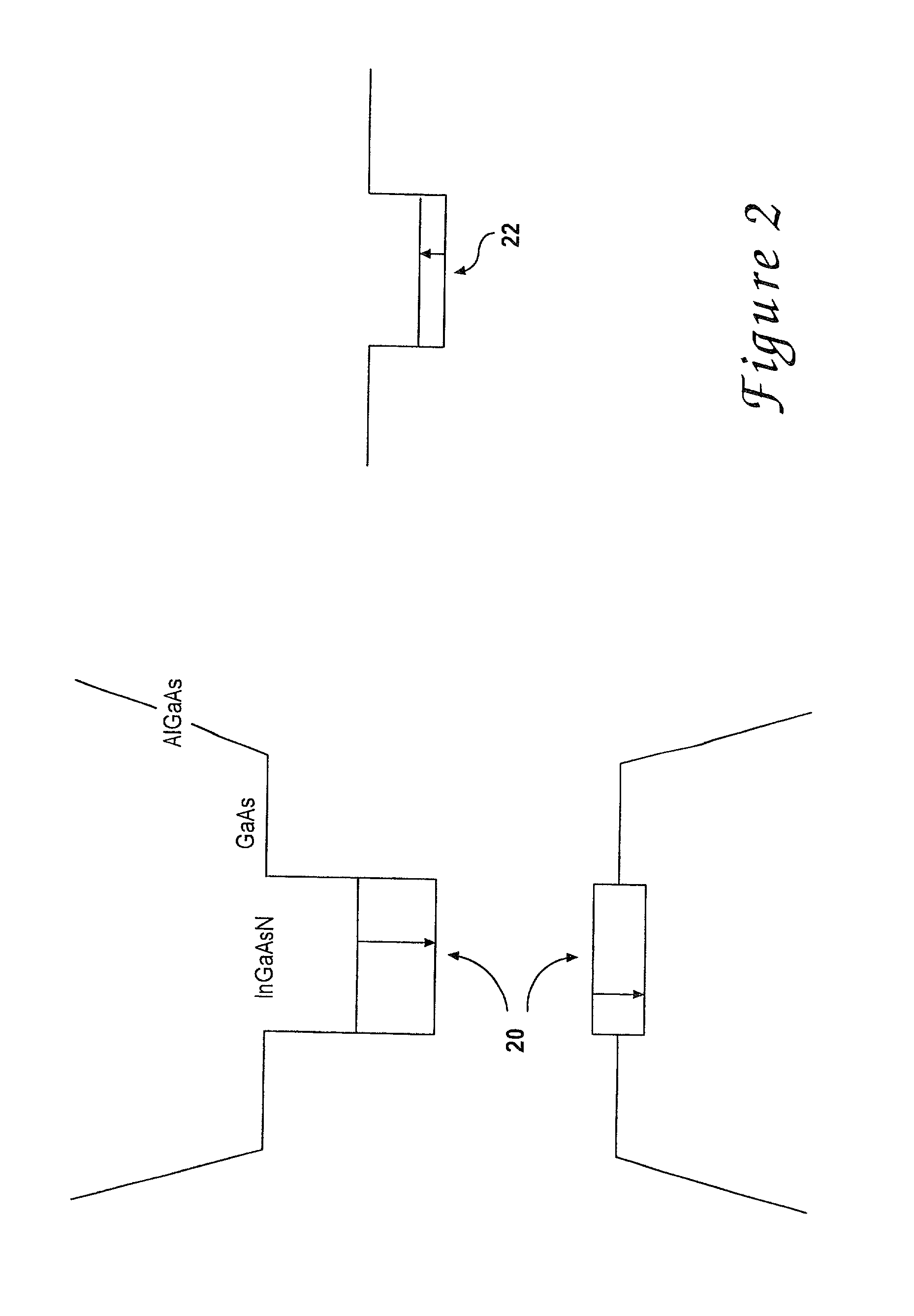
[0051]Making long wavelength quantum wells on GaAs has proven to be very difficult, but technology presented in this the following description has advanced to the point that longer wavelength quantum wells and higher efficiency VCSELs are now feasible. One issue is that long wavelength compounds tend to not be lattice matched to GaAs. This has be...


PUM


Abstract

Quantum wells and associated barriers layers can be grown to include nitrogen (N), aluminum (Al), antimony (Sb), phosphorous (P) and/or indium (In) placed within or about a typical GaAs substrate to achieve long wavelength VCSEL performance, e.g., within the 1260 to 1650 nm range. In accordance with features of the present invention, a vertical cavity surface emitting laser (VCSEL) can include at least one quantum well comprised of InGaAsSbN; barrier layers sandwiching said at least one quantum well; and confinement layers sandwiching said barrier layers. Confinement and barrier layers can comprise AlGaAs. Barrier layer, in the alternative, can also comprise GaAsP. Nitrogen can be placed in the quantum wells. Quantum wells can be developed up to and including 50 Å in thickness. Quantum wells can also be developed with a depth of at least 40 meV.

Description

RELATED APPLICATIONS[0001]The present invention is related to the following co-pending patent applications: Ser. No. 10 / 026,019 entitled “Vertical cavity surface emitting laser including indium and nitrogen in the active region,” filed Dec. 27, 2001; Ser. No. 10 / 026,020 entitled “Vertical cavity surface emitting laser including indium and antinomy in the active region,” filed Dec. 27, 2001; Ser. No. 10 / 026,044 entitled “Indium free vertical cavity surface emitting laser,” filed Dec. 27, 2001; and Ser. No. 10 / 026,055 entitled “Vertical cavity surface emitting laser including indium in the active region,” filed Dec. 27, 2001.TECHNICAL FIELD[0002]This invention relates to vertical cavity surface emitting lasers and more particularly to vertical cavity surface emitting lasers utilizing combinations of nitrogen, aluminum, antimony, phosphorous and / or indium as a material system and as a means to increase VCSEL device wavelength.BACKGROUND OF THE INVENTION[0003]Solid-state semiconductor l...

Claims


Application Information

Patent Timeline
Patent Type & Authority Patents(United States)
IPC IPC(8): H01S5/00H01S5/183H01S5/323H01S5/34H01S5/343
CPCB82Y20/00H01S5/183H01S5/3211H01S5/34353H01S5/32366H01S5/3403H01S5/34306H01S5/32358
Inventor JOHNSON, RALPH H.
Owner II VI DELAWARE INC
Why Eureka
Try Eureka