Computer system and method to dynamically generate system on a chip description files and verification information

a computer system and chip technology, applied in the field of automatic integrated circuit (ic) design, can solve the problems of consuming significant resources, tedious tasks, and complex analysis, and achieve the effects of facilitating the incorporation of building block circuits, facilitating efficient and effective creation, modification and verification, and reducing the amount of data

Inactive Publication Date: 2006-08-29
NXP BV
View PDF8 Cites 98 Cited by
  • Summary
  • Abstract
  • Description
  • Claims
  • Application Information

AI Technical Summary

Benefits of technology

[0008]The present invention is a system and method that facilitates efficient and effective creation, modification and verification of electrical circuit designs utilizing existing circuit block designs. The system on a chip (SoC) netlist builder and verification system and method of the present invention assists a designer to design an integrated circuit (IC) in a convenient manner and facilitates incorporation of building block circuits that have been previously verified and tested in silicon. The SoC netlist builder and verification system and method minimizes the amount of data a user has to enter manually to adequately describe features of the circuit being designed or verified. The present invention system and method automatically provides a chip level netlist description, a test bench, clock descriptions, test logic descriptions, simulation models, and simulation environments.
[0009]In one embodiment of the present invention, an integrated circuit (IC) SoC netlist builder and verification system and method is implemented in a computer system. The SoC netlist builder and verification system and method includes a graphical user interface (GUI), a parameter application module, an expert system module, and a chip level netlist generation module. The GUI module provides user friendly and convenient interfaces that facilitate easy entry and modification of user selections and parameters. In one embodiment the present invention also accommodates text file entry of parameters. The parameter application module analyzes information supplied by the GUI module to interpret the user selections and parameterization (e.g., creates directions (command lines) passed to other modules for execution). The expert system utilizes information derived from past experience designing, manufacturing and verifying circuit blocks to automatically provide circuit block netlist descriptions and parameters from a storage source (e.g., database, distributed resource, memory, etc.). The chip level netlist generation module automatically generates a chip level netlist, including the instantiation of internal IC devices and connections between the circuit blocks for internal signals. In one embodiment of the present invention, an SoC netlist builder and verification system and method also includes a verification module that automatically verifies the behavior of the modeled IC.

Problems solved by technology

Designing complex electronic systems and circuits requires arduous analysis of numerous electrical characteristics, including the performance of extensive calculations and manipulation of complicated electrical principles of physics.
Typically an analysis becomes even more complex when designers attempt to integrate numerous electronic components on a single integrated circuit chip, giving rise to a variety of factors requiring careful review and attention.
Coupling the HDL descriptions of different functional circuit blocks together, generating HDL descriptions of inputs and outputs (IOs) based on the choice of interfaces, adding system level logic for clocking and testing, generating a test bench and the tests to verify the functionality and connectivity of an IC are typically tedious tasks consuming significant resources.
In addition, these design and test activities associated with coupling the different HDL descriptions of functional circuit blocks together are error prone, especially when manual intervention or complex coordination is required.
Valuable experience and information associated with previous design and actual manufacturing of electronic systems is often not available to new design teams.
The new teams of engineers often do not know the circuit block was previously designed, manufactured, tested and debugged and perform these tasks them selves.
Even if the new team includes engineers with experience designing and manufacturing a circuit block, remembering previous designs and circuit block descriptions is often difficult.

Method used


Image

  • Computer system and method to dynamically generate system on a chip description files and verification information
  • Computer system and method to dynamically generate system on a chip description files and verification information
  • Computer system and method to dynamically generate system on a chip description files and verification information

Examples


Embodiment Construction

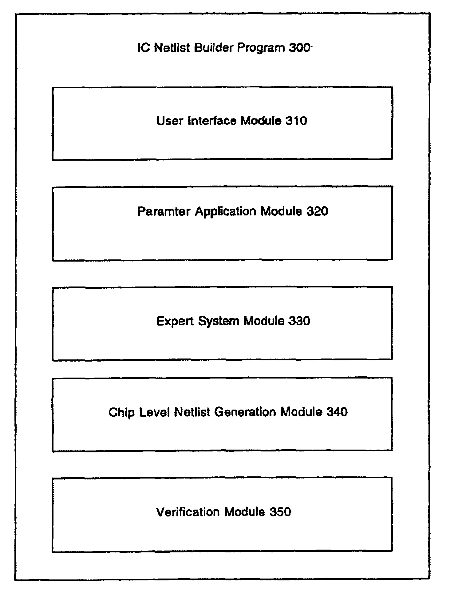
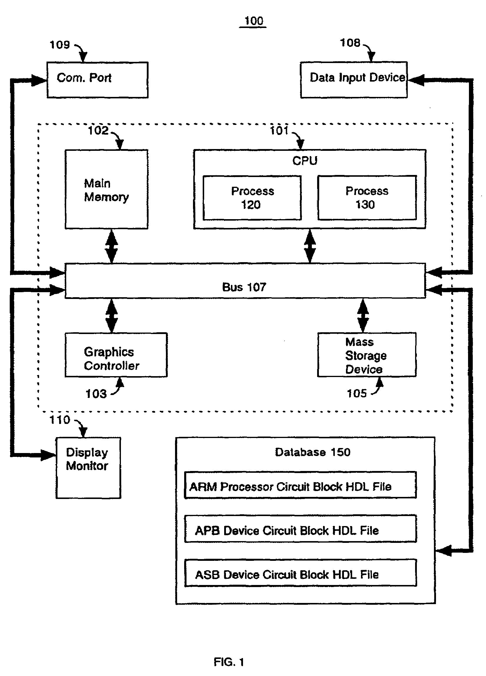
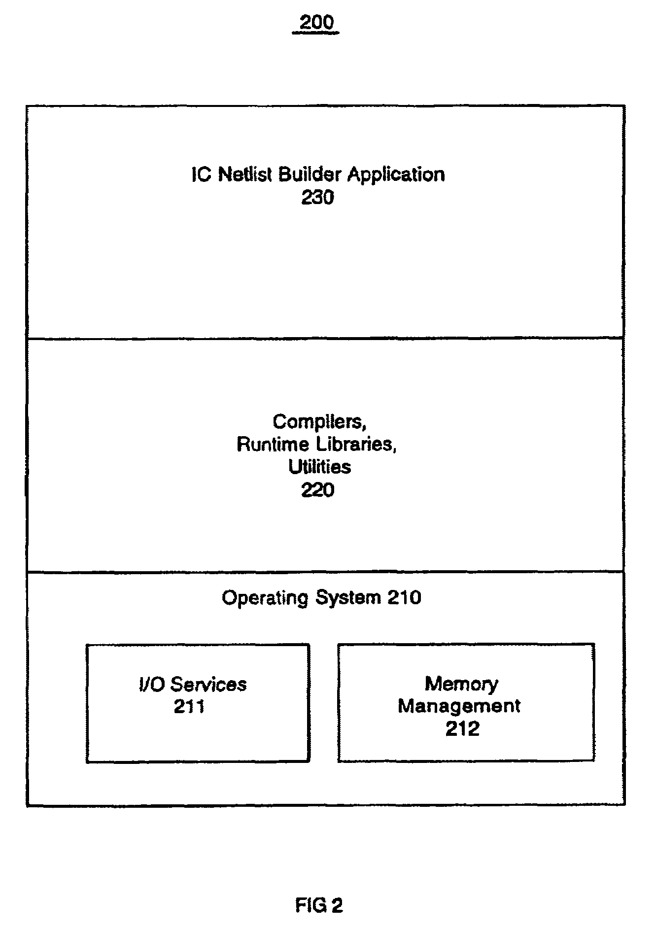
[0032]Reference will now be made in detail to the preferred embodiments of the invention, an IC netlist building system and method, examples of which are illustrated in the accompanying drawings. While the invention will be described in conjunction with the preferred embodiments, it will be understood that they are not intended to limit the invention to these embodiments. On the contrary, the invention is intended to cover alternatives, modifications, and equivalents, which may be included within the spirit and scope of the invention as defined by the appended claims. Furthermore, in the following detailed description of the present invention, numerous specific details are set forth in order to provide a thorough understanding of the present invention. However, it will be obvious to one ordinarily skilled in the art that the present invention may be practiced without these specific details. In other instances, well known methods, procedures, components, and circuits have not been de...


PUM


Abstract

The present invention facilitates automation of system on a chip (SoC) design, manufacture and verification in a convenient and efficient manner. In one embodiment, a SoC netlist builder and verification computer system of the present invention includes a user interface module, a parameter application module, an expert system module and a chip level netlist generation module. The user interface module provides user friendly and convenient interfaces that facilitate easy entry and modification of user selections and parameters. The parameter application module interprets information supplied by the user module and the expert system module and creates directions (e.g., command lines) passed to other modules for execution. The expert system module analyzes information and automatically provides SoC building and verification data including automated addition of default architectural features, automated insertion of default parameters, and automated input of information to the verification module. The chip level netlist generation module automatically generates a chip level netlist, including the instantiation of internal IC devices and connections between the circuit blocks for internal signals. The verification module automatically generates a test bench and a logical verification environment including simulation models (e.g., a chip model and a system level model).

Description

FIELD OF THE INVENTION[0001]The present invention relates to the field of automated integrated circuit (IC) design. More particularly, the present invention relates to system on a chip design and verification system and method that constructs IC hardware description files of systems on a chip from functional building blocks circuits while concurrently taking into account numerous chip level design aspects along with the generation of a simulation environment for design verification.BACKGROUND OF THE INVENTION[0002]Electronic technologies such as digital computers, calculators, audio devices, video equipment and telephone systems have facilitated increased productivity and reduced costs in a number of activities, including the analysis and communication of data, ideas and trends in most areas of business, science, education, and entertainment. There are a number of different complex electronic Application Specific Integrated Circuits (ASICs) that have contributed to the realization o...

Claims


Application Information

Patent Timeline
Patent Type & Authority Patents(United States)
IPC IPC(8): G06F17/50G06F17/00
CPCG06F17/5045G06F17/5022G06F30/30G06F30/33G06F2115/02G06F30/3308
Inventor MEIYAPPAN, SUBRAMANIAN S.VAJJHALA, VARAPRASADPETRYK, EDWARD M.
Owner NXP BV
Why Eureka
Try Eureka