Methods for forming openings in a substrate and apparatuses with these openings and methods for creating assemblies with openings

Inactive Publication Date: 2006-09-05
RUIZHANG TECH LTD CO
View PDF19 Cites 90 Cited by
  • Summary
  • Abstract
  • Description
  • Claims
  • Application Information

AI Technical Summary

Benefits of technology

[0015]The present invention also provides a substrate having at least one opening which is designed to receive an element having a predetermined shape. The element is fabricated separately and assembled into the op

Problems solved by technology

As is well known in the art, it is difficult to produce a completely flawless active matrix liquid crystal display (LCD), when the display area is large, such as the LCD's on modern laptop computers.
Silicon VLSI can be used to produce such an array over a silicon wafer's surface, but silicon wafers are limited in size, limited in conductivity, and not transparent.
Further, processing of large areas on silicon wafers can be expensive.
Single crystal silicon can be bonded to a glass substrate and then etched to remove most of the area to achieve transparency, but this is intrinsically wasteful in that, for the sake of maximizing light transmission, the majority of the processed material is discarded and becomes chemical waste.
The under-utilization of the precious die area wastes resources, causes greater amounts of chemical waste to be generated in the process, and is generally inefficient and expensive.
Large arrays of silicon photodiodes with concentrating lenses have been made by sawing wafers and using a pick and place assembly, but thermal dissipation is poor for large elements, and the small elements require too much assembly time.
These approaches avoid the limitations of the size of the available single crystal silicon wafers, and avoid the cost of the single crystal wafers, but require expensive deposition of the semiconductor layer, and they still require processing of the entire large substrate to form the active elements in an array, still resulting in the production of much chemical waste and wasted resources.
These processes also limit the choice of the substrate; for example, plastic substrates cannot be used due to the nature of the processes which deposit the semiconductor layers.
F

Method used


Image

  • Methods for forming openings in a substrate and apparatuses with these openings and methods for creating assemblies with openings
  • Methods for forming openings in a substrate and apparatuses with these openings and methods for creating assemblies with openings
  • Methods for forming openings in a substrate and apparatuses with these openings and methods for creating assemblies with openings

Examples


Example

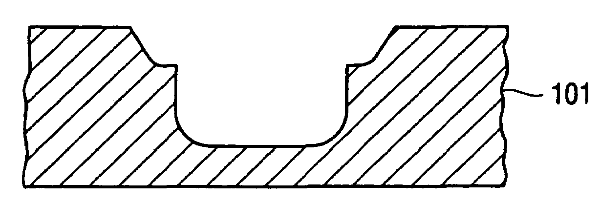
[0038]The present invention relates to methods and apparatuses for forming openings in a receiving substrate. The following description and drawings are illustrative of the invention and are not to be construed as limiting the invention. Numerous specific details are described to provide a thorough understanding of the present invention. However, in certain instances, well known or conventional details are not described in order to not unnecessarily obscure the present invention in detail.

[0039]The present invention relates generally to the field of creating openings in a receiving substrate and to apparatuses having these openings. The present invention may be used to fabricate openings for various different types of arrays. Typically, each element in the array includes a functional component which may be an electrical component, a chemical component, or an electromechanical structural element or a micro electromechanical structural element or a micro-mechanical structural element....


PUM

PropertyMeasurementUnit
Lengthaaaaaaaaaa
Lengthaaaaaaaaaa
Structureaaaaaaaaaa

Abstract

Methods for forming openings having predetermined shapes in a substrate and apparatuses with these openings. The methods may be used to form assemblies which include the substrate with its openings and elements which are disposed in the openings. In one example of a method, each of the elements include an electrical component and are assembled into one of the openings by a fluidic self assembly process. In an particular example of a method to create such an opening, the substrate is etched through a first patterned mask and is later etched through a second patterned mask. Typically, the second patterned mask is aligned relative to the opening created by etching through the first patterned mask and has an area of exposure which is smaller than an area of exposure through the first patterned mask. In another example of a method, a photosensitive material is exposed through a patterned mask to oblique sources of light such that some of the light impinges into a first portion of the photosensitive material which is under the patterned mask, and the patterned mask and a second portion of the photosensitive material, which is under the patterned mask, is removed. In another example of a method, an opening in a first layer, which comprises silicon dioxide, is formed by depositing a second layer over the first layer and depositing a tungsten layer over the second layer. The tungsten and second layers are patterned to expose a portion of the first layer, and this portion is etched. Various apparatuses which may be made using these methods are also described.

Description

RELATED APPLICATIONS[0001]This is a continuation of application Ser. No. 09 / 432,512, filed on Nov. 2, 1999 now U.S. Pat. No. 6,479,395.FIELD OF THE INVENTION[0002]The present invention relates generally to the field of fabricating openings in a substrate and also to apparatuses with these openings. More particularly, the present invention relates to methods for forming openings in a substrate which openings are designed to receive an element which is later placed into the opening and which element includes at least one functional component, and the present invention relates to methods for creating assemblies with the openings.BACKGROUND OF THE INVENTION[0003]There are many examples of large arrays of functional components which can provide, produce or detect electromagnetic signals or chemicals or other characteristics. An example of such a large array is that of a display where many pixels or sub-pixels are formed on an array of electronic elements. For example, an active matrix li...

Claims


Application Information

Patent Timeline
IPC IPC(8): B28B11/00B81C1/00G02F1/1362H01L21/027H01L21/308H01L21/311H01L21/48H01L23/538
CPCB81C1/00357G02F1/1362H01L21/0274H01L21/3065H01L21/3083H01L21/31144H01L21/4803H01L23/5389H01L24/24H01L24/31H01L24/82H01L24/95H01L24/97B81C1/00428Y10S977/883B81C2201/019B82Y30/00G02F2001/136295H01L2224/24225H01L2224/24227H01L2224/95085H01L2224/95092H01L2224/95122H01L2224/95136H01L2224/95144H01L2224/97H01L2924/01005H01L2924/01011H01L2924/01013H01L2924/01027H01L2924/01047H01L2924/01074H01L2924/01082H01L2924/10158H01L2924/10253H01L2924/14H01L2924/15153H01L2924/15155H01L2924/15157H01L2924/15165H01L2924/15788H01L2924/19041H01L2924/19042H01L2924/19043H01L2924/12041H01L2924/01084H01L2924/01072H01L2924/01033H01L2924/01019H01L2224/32225H01L2924/01006H01L2224/82G02F1/136295H01L2924/12042H01L2924/12043H01L2924/00
Inventor SMITH, JOHN STEPHENHADLEY, MARK A.CRAIG, GORDON S. W.LOWE, FRANK
Owner RUIZHANG TECH LTD CO
Why Eureka
Try Eureka