End of range (EOR) secondary defect engineering using substitutional carbon doping

a substitutional carbon and secondary defect technology, applied in semiconductor devices, single crystal growth, chemistry apparatus and processes, etc., can solve the problems of end of range (eor) secondary defect formation at the tail end of the profile, excessive dopant diffusion, and high cost, so as to prevent transient enhanced diffusion of indium, prevent and prevent the effect of end of range secondary defect formation

Inactive Publication Date: 2006-09-19
TAIWAN SEMICON MFG CO LTD
View PDF9 Cites 101 Cited by
  • Summary
  • Abstract
  • Description
  • Claims
  • Application Information

AI Technical Summary

Benefits of technology

[0008]Accordingly, a primary object of the invention is to provide a method to prevent formation of EOR secondary defects in the fabrication of integrated circuits.
[0009]A further object of the invention is to provide a method to prevent formation of EOR secondary defects in connection with an indium halo implant.
[0010]Another object of the invention is to provide a method to prevent formation of EOR secondary defects in connection with an indium halo implant through the presence of substitutional carbon acting as a silicon interstitial sink.

Problems solved by technology

The indium ion has large cross-sectional area and, when implanted at high energy, causes much damage to the silicon lattices compared to its boron counterpart.
This causes formation of the End of Range (EOR) secondary defect at the tail end of the profile upon insufficient annealing.
A prolonged soak anneal would cause unnecessary dopant diffusion, undesirable for shallow junction formation.
EOR defects when present in the depletion region of the PN junction cause severe junction leakage.
The implantation of carbon itself introduces additional silicon interstitials, reducing the effectiveness of carbon as a sink.

Method used


Image

  • End of range (EOR) secondary defect engineering using substitutional carbon doping
  • End of range (EOR) secondary defect engineering using substitutional carbon doping
  • End of range (EOR) secondary defect engineering using substitutional carbon doping

Examples


Embodiment Construction

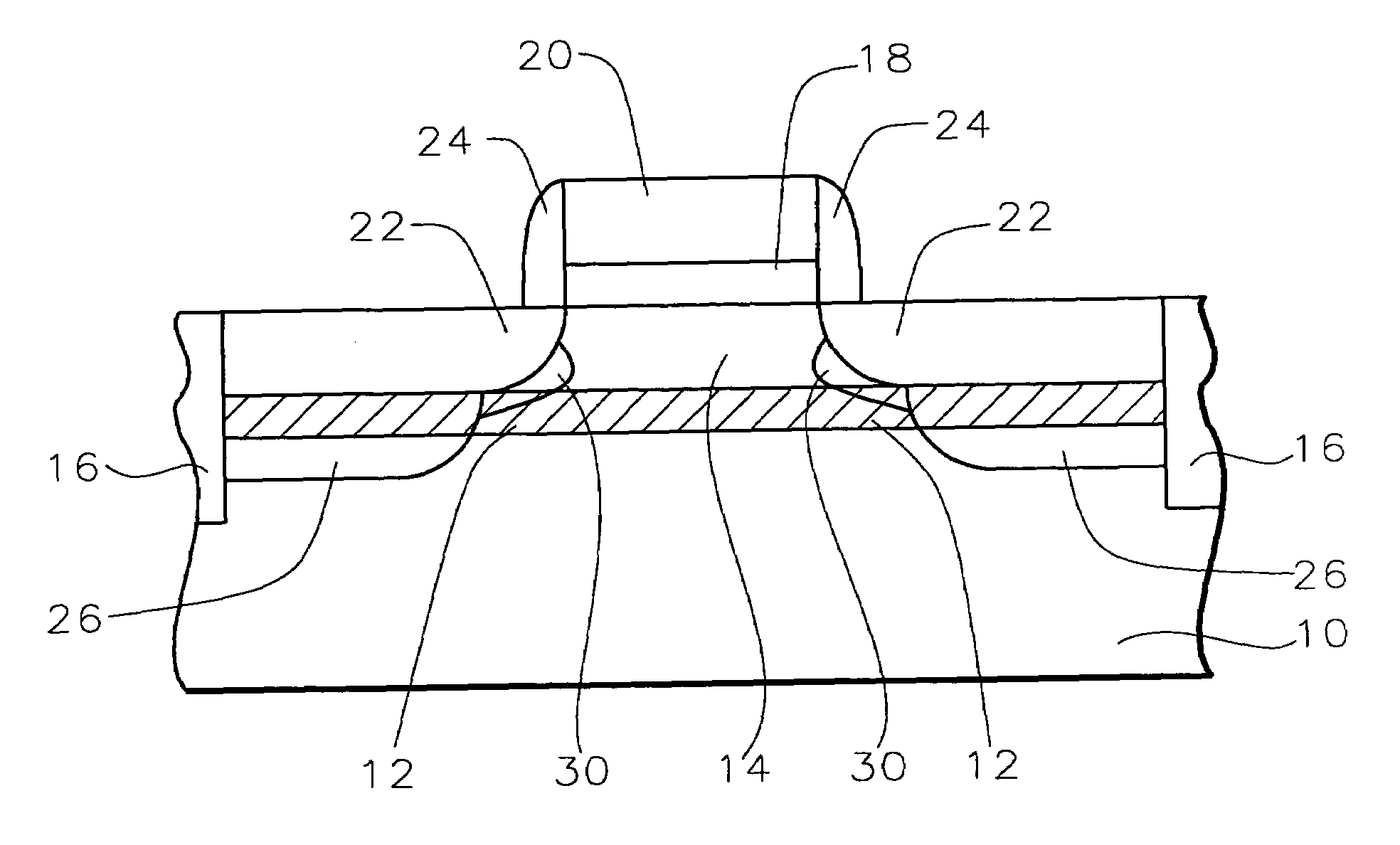
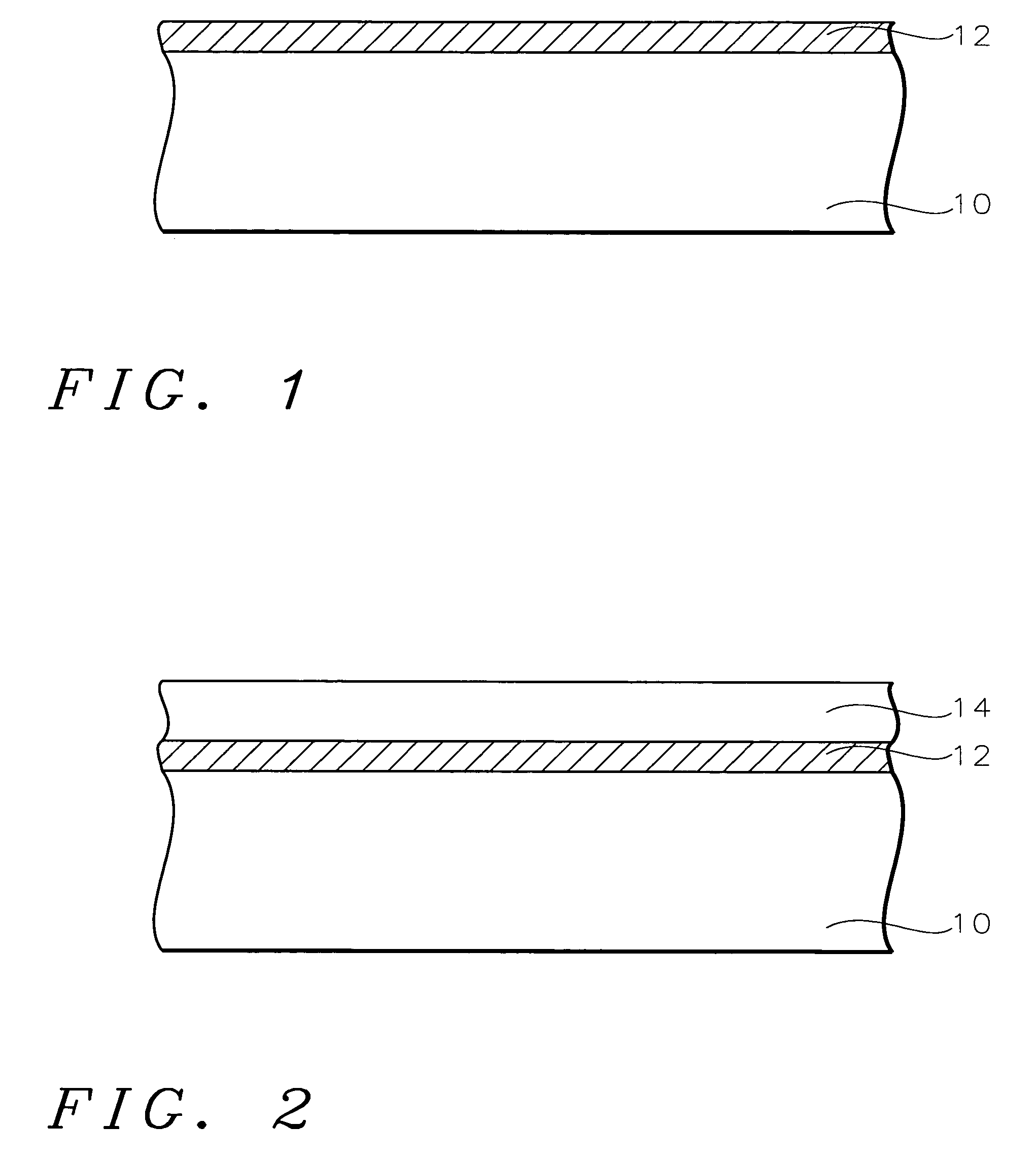
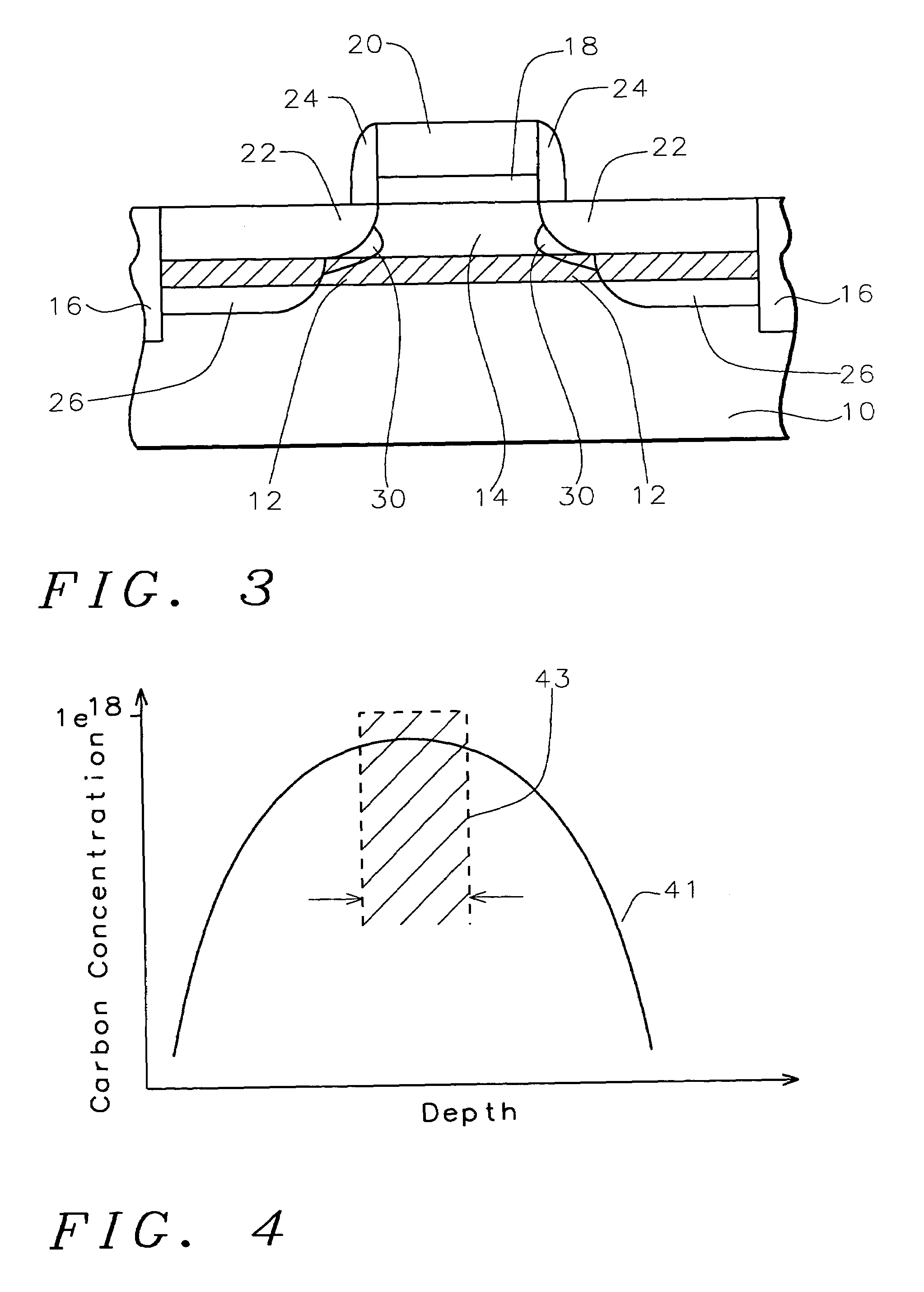
[0022]The present invention introduces a layer of substitutional carbon to the tail end of the halo doping profile in order to reduce the secondary defect formation due to the indium halo doping implantation. It is a simple process, yet superior to carbon co-implantation as no additional implant damage is introduced through this method.

[0023]A carbon implant by itself would inherently cause damage at the tail end of the implantation profile. This causes additional damage which can be avoided if the carbon is doped using the CVD method. Carbon doped by this method is substitutional and does not require an additional annealing process. FIG. 4 illustrates the carbon implant profile 41 of the prior art methods where carbon is implanted into silicon. The profile 41 is a skewed gaussian-like distribution. Moreover, the smaller carbon atoms diffuse very fast making it difficult to control the profile. Using the RPCVD method of the present invention, a much more precise and accurate doping ...


PUM

PropertyMeasurementUnit
thicknessaaaaaaaaaa
thicknessaaaaaaaaaa
thicknessaaaaaaaaaa

Abstract

A method for incorporating carbon into a wafer at the interstitial a-c silicon interface of the halo doping profile is achieved. A bulk silicon substrate is provided. A carbon-doped silicon layer is deposited on the bulk silicon substrate. An epitaxial silicon layer is grown overlying the carbon-doped silicon layer to provide a starting wafer for the integrated circuit device fabrication. An integrated circuit device is fabricated on the starting wafer by the following steps. A gate electrode is formed on the starting wafer. LDD and source and drain regions are implanted in the starting wafer adjacent to the gate electrode. Indium is implanted to form halo implants adjacent to the LDD regions and underlying the gate electrode wherein the halo implants extend to an interface between the epitaxial silicon layer and the carbon-doped silicon layer wherein carbon ions in the carbon-doped silicon layer act as a silicon interstitial sink for silicon interstitials formed by the halo implants to prevent end of range secondary defect formation.

Description

BACKGROUND OF THE INVENTION[0001](1) Field of the Invention[0002]The present invention relates to the fabrication of integrated circuit devices, and more particularly, to a method of reducing secondary defect formation due to indium halo doping in the fabrication of integrated circuits.[0003](2) Description of the Prior Art[0004]Halo or pocket implants are made in the fabrication of integrated circuits in order to suppress n-channel and p-channel short channel effects, to suppress drain-induced-barrier-lowering, and to suppress high electrical field regions that could cause punchthrough phenomenon. The use of heavy ions (e.g. antimony or indium) as a dopant for the halo pocket of the nMOSFET becomes more important with the shrinkage of the nMOS transistor to below the sub-0.1 μm regime. See “Optimum Halo Structure for Sub-0.1 μm CMOSFETs”, Wen-Kuan Yeh, IEEE Transaction on Electron Devices, Vol. 48, No. 10, October 2001 and “Antimony Assisted Arsenic S / D Engineering for sub-0.1 μm n...

Claims


Application Information

Patent Timeline
Patent Type & Authority Patents(United States)
IPC IPC(8): H01L21/425H01L21/20H01L21/265H01L21/36C30B1/00H01L21/336H01L21/74H01L29/10
CPCH01L21/02381H01L21/02447H01L21/02532H01L29/6659H01L21/74H01L29/1054H01L21/26513H01L21/26506
Inventor TAN, CHUNG FOONGLIU, JINPINGLEE, HYEOK JAEINDAJANG, BANGUNCHOR, ENG FONGONG, SHIANG YANG
Owner TAIWAN SEMICON MFG CO LTD
Why Eureka
Try Eureka