Optical element assembly and method of making the same

Inactive Publication Date: 2006-09-19
JAPAN AVIATION ELECTRONICS IND LTD
View PDF11 Cites 7 Cited by
  • Summary
  • Abstract
  • Description
  • Claims
  • Application Information

AI Technical Summary

Benefits of technology

[0017]Since the optical element assembly of the present invention has the above-mentioned configuration in which the optical element is positioned on the mounting surface of the platform and the optical element is automatically positioned by the part receiving concavity with respect to the mounting surface, optical coupling between the optical part and the optical element is established with high accuracy. That is, since the optical element is formed on the protruding end face of the convexity or on the bottom of the concavity of the optical element chip, it is possible to adopt techniques of simultaneously forming a large number of convexities or concavities in a w

Problems solved by technology

However, since light inlet and outlet ports of such a slab type photonic crystal optical waveguide are approximately 1 μm or less in size (in thickness) that is smaller than the core diameter (about 4 to 10 μm in single mode) of an optical fiber, high-precision positioning of the waveguide and the optical fiber is difficult to achieve—this constitutes an obstacle to high-efficiency input of light to the waveguide.
In the case of the optical waveguide of the photonic crystal having air holes periodically arranged in the high refractive index material layer, since light is launched into the layer from air, reflectivity on the plane of incidence is high, giving rise to a heavy coupling loss.
It is difficult to mount such a microminiature optical element as the photonic crystal element by the

Method used


Image

  • Optical element assembly and method of making the same
  • Optical element assembly and method of making the same
  • Optical element assembly and method of making the same

Examples


embodiment 1

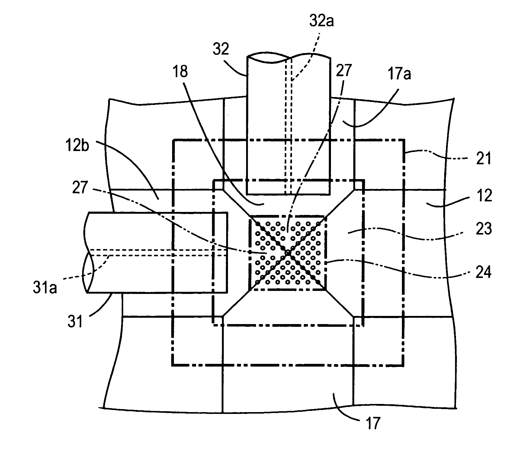
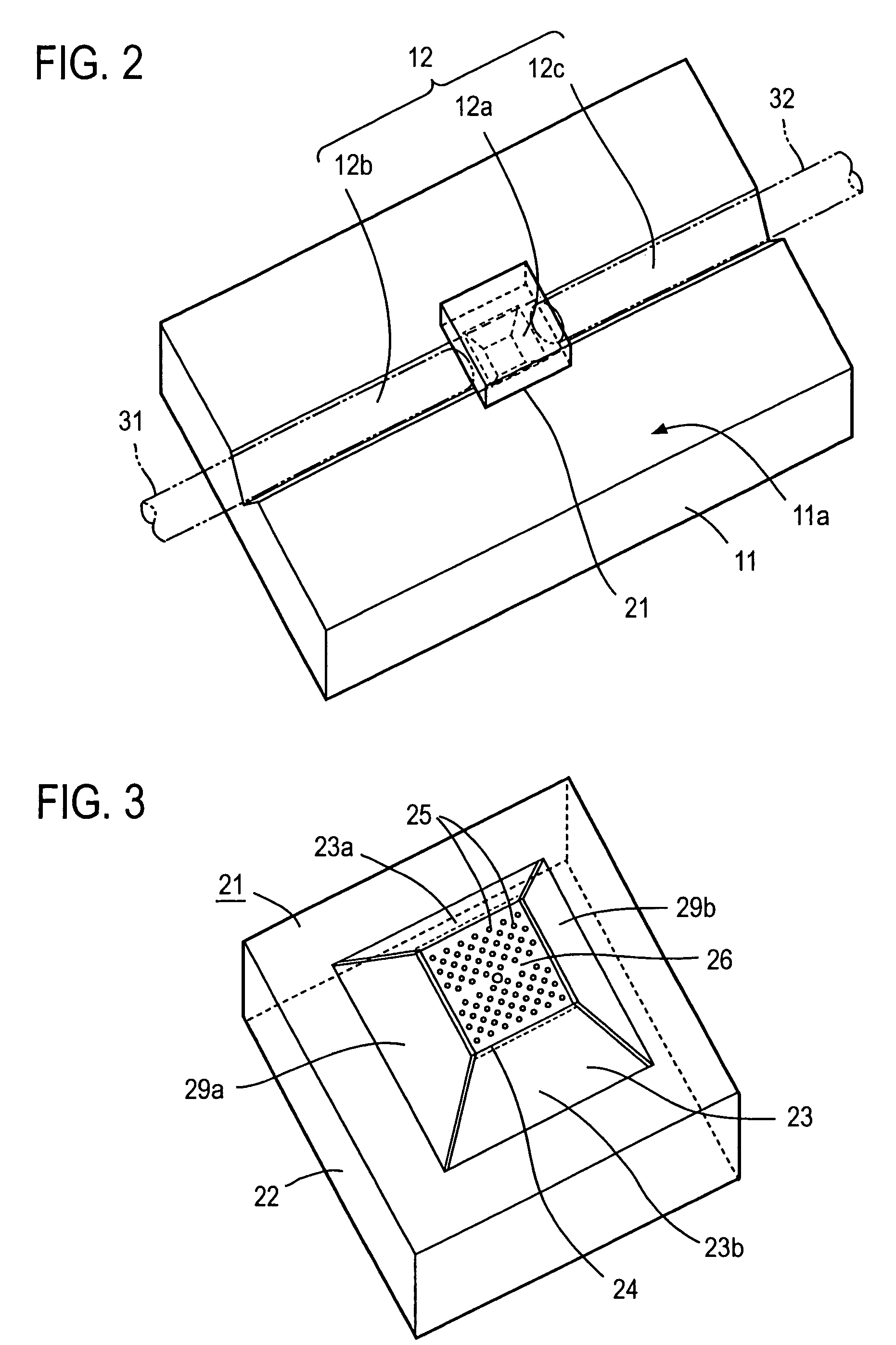
[0047]This embodiment uses, as an optical element, a wavelength filter formed of a photonic crystal. As depicted in FIG. 2, an optical element chip 21 is positioned with respect to the mounting surface 11a and mounted on an element mounting portion 12a formed in one surface, i.e. in a mounting surface of a platform 11. The optical element chip 21 may be adhesively bonded to the platform 11. In this embodiment the platform 11 has in its mounting surface 11a a V-groove 12 extending from the one to the other end thereof, and the intermediate portion of the V-groove 12 is used as the element mounting portion 12a. The V-groove portions 12 at both sides of the element mounting portion 12a form part receiving recesses 12b and 12c; in this example, optical fibers 31 and 32 as optical parts are inserted in the part receiving recesses 12b and 12c, then positioned with respect to the mounting surface 11a, and fixed to the platform 11. The optical fibers 31 and 32 are, for example, adhesively b...

embodiment 2

[0068]This embodiment is intended to increase the number of optical element chips 21 obtainable from one wafer 20 (FIG. 6) by making the width of the V-grove of the element mounting portion 12a narrower than the part receiving recesses 12b and 12c and reducing the length of protrusion of the convexity 23. FIG. 7 shows an example of the platform 11 in this embodiment. The element mounting portion 12a and the part receiving recesses 12b and 12c formed by V-grooves are axially aligned with each other, looking in the direction perpendicular to the mounting surface 11a, but the groove width W3 of the element mounting portion 12a is smaller than the groove width W4 of each of the part receiving recesses 12b and 12c. In the case of forming theses V-grooves by anisotropic etching, since both ends of the element mounting portion 12a protrude obliquely downwardly into the recesses 12b and 12c, the optical fibers 31 and 32 cannot be disposed close to the optical element 24 accordingly. In this...

embodiment 3

[0070]This embodiment uses a microminiature lens as an optical part. FIG. 10 shows in section the structure of this embodiment, corresponding to the FIG. 4 sectional view of Embodiment 1, and FIG. 11 depicts an example of the platform 11 for use in this embodiment. In the mounting surface 11a of the platform 11 there are formed a square part receiving concavity 14 and a V-groove 15 extending at right angles to one side thereof and opening into the concavity 14. One part 15a of the V-groove 15 is used as the element mounting portion. In this example, the V-groove 15 is formed as its extension 15b in the platform surface also on the side thereof opposite the element mounting portion 15a; that is, the V-groove 15 opens at both ends to the outside of the platform 11. The part receiving concavity 14 and the V-groove 15 can be formed simultaneously by, for example, anisotropic etching.

[0071]As shown in FIG. 10, a microminiature spherical lens 33 is disposed in and positioned by the part r...


PUM


Abstract

A V-groove is formed in a platform of single crystal silicon by anisotropic wet etching based on its crystal orientation, and a convexity of an optical element chip is fitted in an intermediate portion of the V-groove. Quadrangular frustoidal convexities are formed in rows and columns on a single crystal silicon wafer by anisotropic wet etching, then a photonic crystal filter element is formed as an optical element on the protruding end face of each convexity, and the wafer is cut for each optical element into individual optical element chips. When optical fibers are disposed in the V-groove at both sides of the chip, cores of the optical fibers and light inlet and outlet ports of the optical element are aligned with each other.

Description

BACKGROUND OF THE INVENTION[0001]The present invention relates to an optical element assembly for use, for example, in the fields of optical communications, which permits highly accurate positioning of a microminiature optical element, such as a photonic crystal optical element, and an optical part, such as an optical fiber, with respect to each other. The invention also pertains to a method for the manufacture of such an optical element assembly.[0002]In the fields of optical communications, a lot of attention has recently been given to artificial crystal materials (photonic crystals) whose refractive index changes with a period on the order of light wavelength. With the use of such photonic crystals, it is expected that advanced light-controlled functional elements which were impossible to realize in the past, such as a low-loss macrobend waveguide, a low-threshold laser and a wavelength division multiplexing element, can be fabricated in sizes of 100 μm×100 μm or smaller. With ra...

Claims


Application Information

Patent Timeline
IPC IPC(8): G02B6/12G02B6/26G02B6/122G02B6/136G02B6/36G02B6/42
CPCB82Y20/00G02B6/12004G02B6/1225G02B6/136G02B6/3692G02B6/4214G02B2006/12176G02B6/3652G02B6/3636
Inventor SUZUKI, AKIKO
Owner JAPAN AVIATION ELECTRONICS IND LTD
Why Eureka
Try Eureka