Passivation of material using ultra-fast pulsed laser

a pulsed laser and ultra-fast technology, applied in the direction of basic electric elements, electrical equipment, semiconductor devices, etc., can solve the problems of reducing the efficiency of radio-frequency (rf) and wireless communication applications, affecting the efficiency of semiconductor devices, and affecting the efficiency of radio-frequency (wiii) communications

Inactive Publication Date: 2006-09-26
THE BOARD OF TRUSTEES OF THE UNIV OF
View PDF10 Cites 32 Cited by
  • Summary
  • Abstract
  • Description
  • Claims
  • Application Information

AI Technical Summary

Benefits of technology

[0010]The problem of passivating the surface of a semiconductor substrate, such as gallium arsenide and the like, has now been alleviated by the process of the invention wherein the surface of a substrate material is irradiated with one

Problems solved by technology

However, silicon also has certain limitations, particularly in the field of wireless communications, especially as higher frequencies have come into use.
Because silicon has an indirect band gap structure, it is less efficient for applications involving radio-frequency (RF) and wireless communications.
Consequently, GaAs semiconductor devices, although generally more expensive, have found a commercially valuable niche where silicon cannot effectively compete.
However, manufacture of semiconductor devices from GaAs also faces some challenges.
Most importantly, unlike Si, GaAs does not form a natural and stable protective passivating layer.
Consequently, it has been difficult to design and manufacture m

Method used


Image

  • Passivation of material using ultra-fast pulsed laser
  • Passivation of material using ultra-fast pulsed laser
  • Passivation of material using ultra-fast pulsed laser

Examples


example

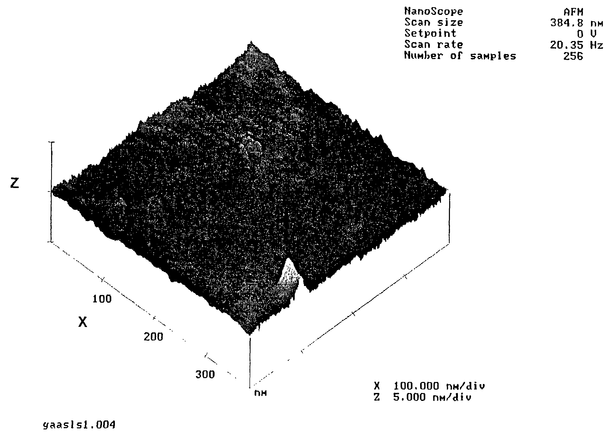
[0038]This example illustrates the treatment of a gallium arsenide surface to remove the naturally existing surface oxide and prepare a stable passive surface.

[0039]Samples of n(100) GaAs, 600 micrometers thick, were prepared. Each sample was about 1 cm×1 cm in dimensions, and was degreased by treating it with warm methanol for about two minutes. The samples were then rinsed in flowing de-ionized water and dried in flowing nitrogen gas. The cleaned GaAs samples were mounted vertically on a computer controlled X-Y-Z translation stage.

[0040]The samples were then treated with an unfocussed femtosecond laser beam. The laser treatment was performed in air in an effort to make the laser treatment as representative as possible of conventional environmental conditions in the semiconductor industry. The laser was an excimer pumped UV-dye laser having a wavelength of about 248 nm, a pulse duration of about 380 femtoseconds (fs), and an output energy of about 10 millijoules (mJ) per pulse, wit...


PUM


Abstract

The surface of a semiconductor material, e.g., gallium arsenide, is passivated by irradiating the surface with ultra-short laser pulses, until a stable passive surface is achieved. The passive surface so prepared is devoid of a superficial oxide layer.

Description

CROSS-REFERENCE TO RELATED APPLICATION[0001]This application claims the benefit of the priority of U.S. Provisional Application No. 60 / 153,069, filed Sep. 10, 1999, the entire disclosure of which is incorporated herein by reference.BACKGROUND OF THE INVENTION[0002]1. Field of the Invention[0003]This invention relates to forming passivated surfaces on solid materials and more particularly to formation of passivated surfaces on semiconductor materials by laser irradiation.[0004]2. Brief Description of the Prior Art[0005]The design and manufacture of semiconductor devices is based on the electronic properties of the bulk semiconductor material of which they are made. The bulk material is ordinarily a single crystal having a uniform lattice structure and containing various dopants, which introduce the impurity levels required to provide the desired electrical conduction properties. Within the bulk crystal each atom is bound to its neighbors in the lattice. However, at the surface of the...

Claims


Application Information

Patent Timeline
IPC IPC(8): H01L21/26
CPCH01L21/268H01L21/302Y10S438/974Y10S438/958
Inventor RAILKAR, TARAK A.MALSHE, AJAY P.BROWN
Owner THE BOARD OF TRUSTEES OF THE UNIV OF
Why Eureka
Try Eureka