
Eureka
For R&D, Eureka makes reading and utilizing patents & technical documents easy.
Eureka AIR
Designed for self-driven R&D workflows. Generate viable solutions, solve complex R&D challenges, empower your innovation with AI.

Eureka Materials
Designed for material experts only. Revolutionize your material R&D, from search, analyze, to developing new materials.

TechResearch
Generate reliable direction feasibility study reports for your R&D in just a few steps.

TechSeek
Discover and master advanced knowledge NOW. Basics, ideas, possibilities, all at once.

TechMind
As an expert in R&D Theories, TechMind can generates customized viable solutions instantly.

TechRisk
Analyze your overall solution with one click, know your potential R&D risks in advance.

TechMonitor
Get weekly tech updates, stay abreast of the latest tech innovations and key insights.
Gate with dual gate dielectric layer and method of fabricating the same
- Summary
- Abstract
- Description
- Claims
- Application Information
AI Technical Summary
Problems solved by technology
Method used
Image

Examples
Embodiment Construction
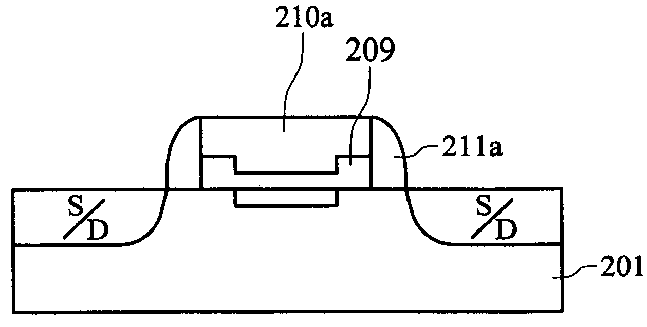
[0021]FIGS. 2a to 2l are cross-sections of the method for fabricating a MOS with dual gate dielectric layer of the present invention.
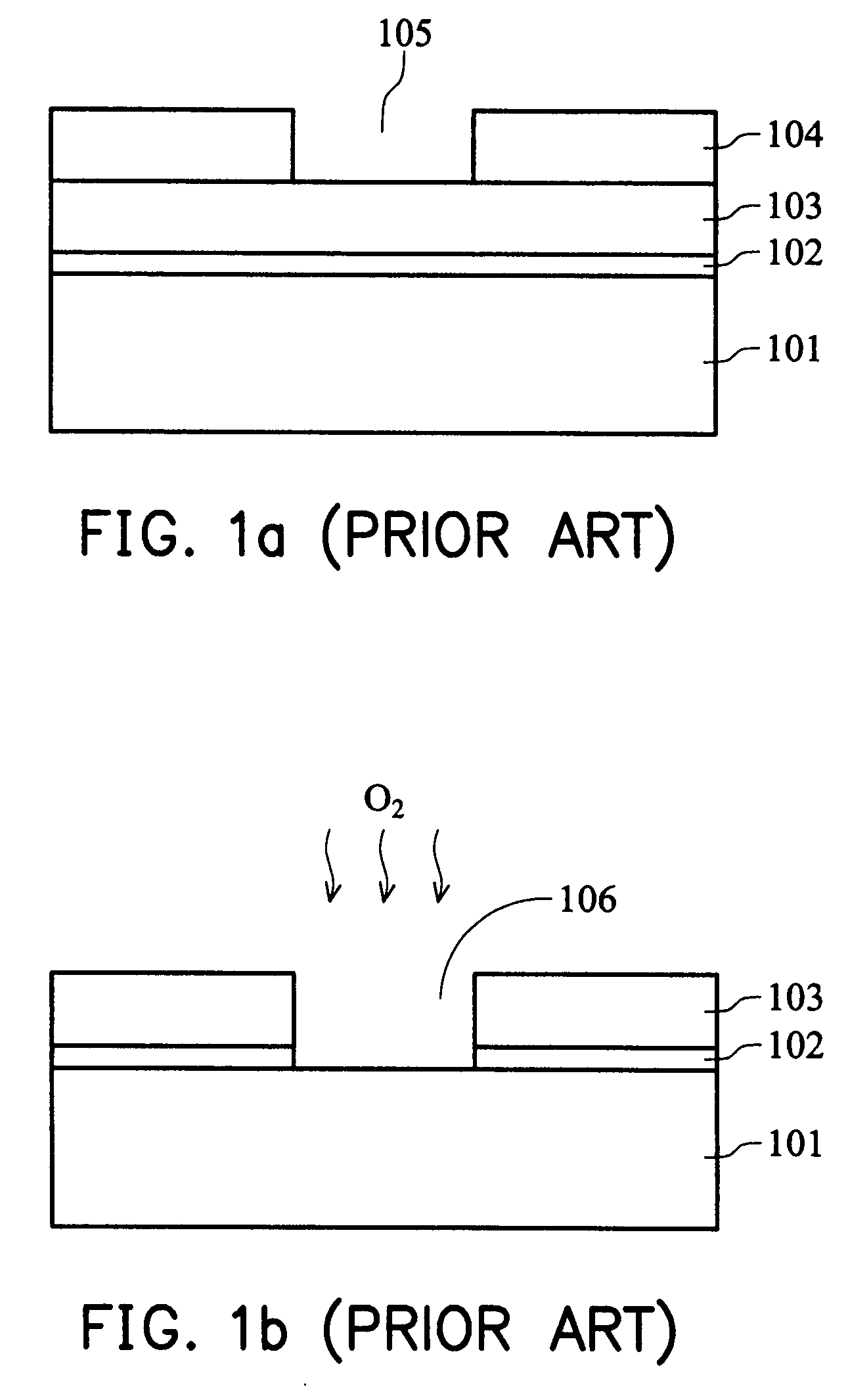
[0022]In FIG. 2a, a semiconductor substrate 201, such as silicon substrate, is provided, on which a dielectric layer 202, such as pad oxide layer, a hard mask layer 203, such as LPCVD nitride layer, and a patterned photoresist layer 204 with an opening 205 are sequentially formed. The LPCVD nitride layer is deposited using SiCl2H2 and NH3 as reactive gas at 250 to 400° C. The position of the opening 205 is the position of a dual gate dielectric layer in the subsequent process, and the opening 205 exposes the surface of the hard mask layer 203.
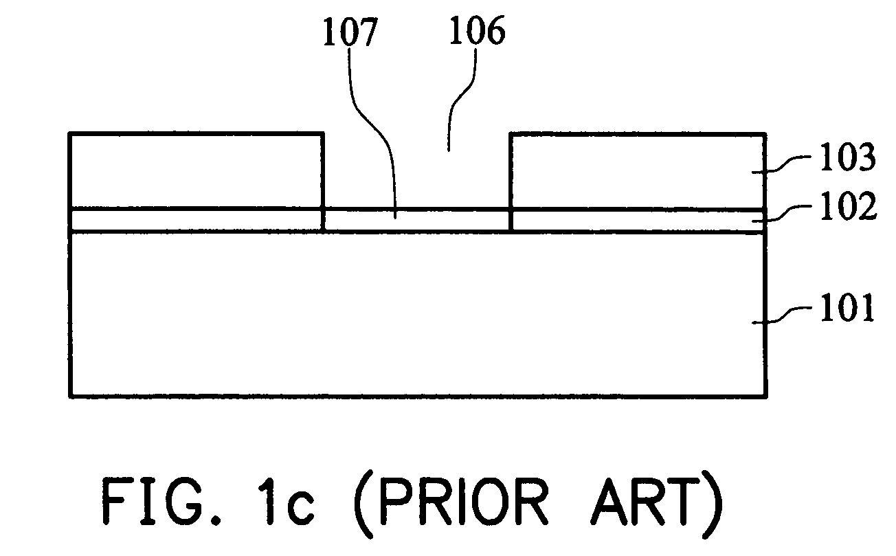
[0023]In FIG. 2b, the hard mask layer 203 is etched using the patterned photoresist layer 204 to form an opening in the hard mask layer 203, wherein the opening exposes the surface of the semiconductor substrate 201.
[0024]In FIG. 2c, a first insulating layer 207, such as LPCVD oxide layer or PECVD oxide layer, is ...
PUM
 Abstract
Description
Claims
Application Information
 - R&D Engineer
- R&D Manager
- IP Professional
- Industry Leading Data Capabilities
- Powerful AI technology
- Patent DNA Extraction
Browse by: Latest US Patents, China's latest patents, Technical Efficacy Thesaurus, Application Domain, Technology Topic, Popular Technical Reports.
© 2024 PatSnap. All rights reserved.Legal|Privacy policy|Modern Slavery Act Transparency Statement|Sitemap|About US| Contact US: help@patsnap.com