Dynamic random access memory and fabrication thereof

a random access memory and dynamic technology, applied in the field of dynamic random access memory cell and array structure, can solve the problem of more difficult filling of cracks, and achieve the effect of increasing the surface area of capacitors

Inactive Publication Date: 2006-10-10
PROMOS TECH INC
View PDF1 Cites 6 Cited by
  • Summary
  • Abstract
  • Description
  • Claims
  • Application Information

AI Technical Summary

Benefits of technology

[0007]In view of the foregoing, one aspect of this invention is to provide a DRAM cell that has a capacitor formed on the sidewall of a semiconductor pillar to eliminate the trench-filling problem in the prior art and to increase capacitor surface area.
[0009]Still another aspect of this invention is to provide a method for fabricating a DRAM array, so as to eliminate the trench-filling problem in the prior art, to increase the capacitance of the capacitor, and to increase the integration of DRAM devices.
[0014]Since the capacitor in a DRAM cell of this invention is formed around a semiconductor pillar, but not in a deep trench, the trench-filling problem in the prior art due to the high aspect ratio of deep trenches is thus obviated. Meanwhile, the surface area / capacitance of the capacitor is quite large, because the capacitor can be formed on all sides of the pillar and the second plate as an upper electrode is inserted between the first plate and the third plate to further double the capacitance.
[0015]Moreover, since the transistor of a DRAM cell of this invention is formed with a vertical structure, the lateral area occupied by a memory cell can be significantly reduced to remarkably increase the integration of a DRAM array. In other words, the DRAM array of this invention can have a higher degree of integration.
[0016]Furthermore, since a capacitor is formed around a semiconductor pillar in the method for fabricating a DRAM array of this invention, the trench-filling problem in the prior art is precluded. Therefore, the quality of the storage capacitors can be improved.

Problems solved by technology

As the aspect ratio becomes higher, for example, exceeds 20:1, the trench becomes more difficult to fill.

Method used


Image

  • Dynamic random access memory and fabrication thereof
  • Dynamic random access memory and fabrication thereof
  • Dynamic random access memory and fabrication thereof

Examples


Embodiment Construction

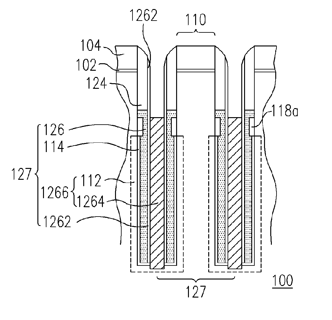
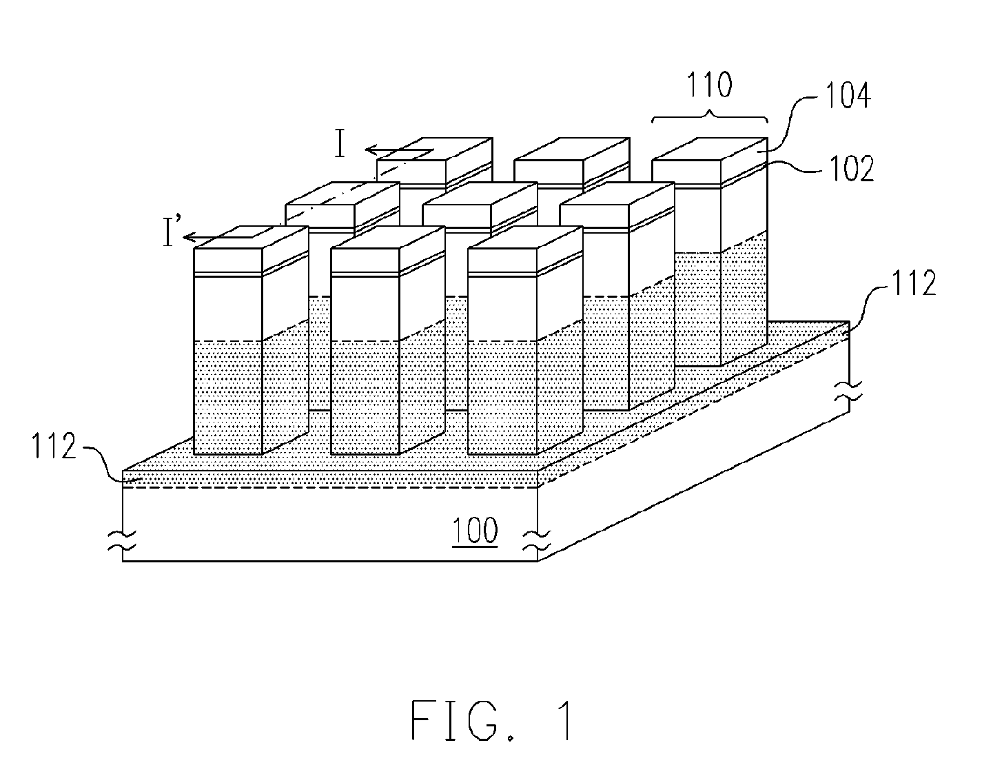
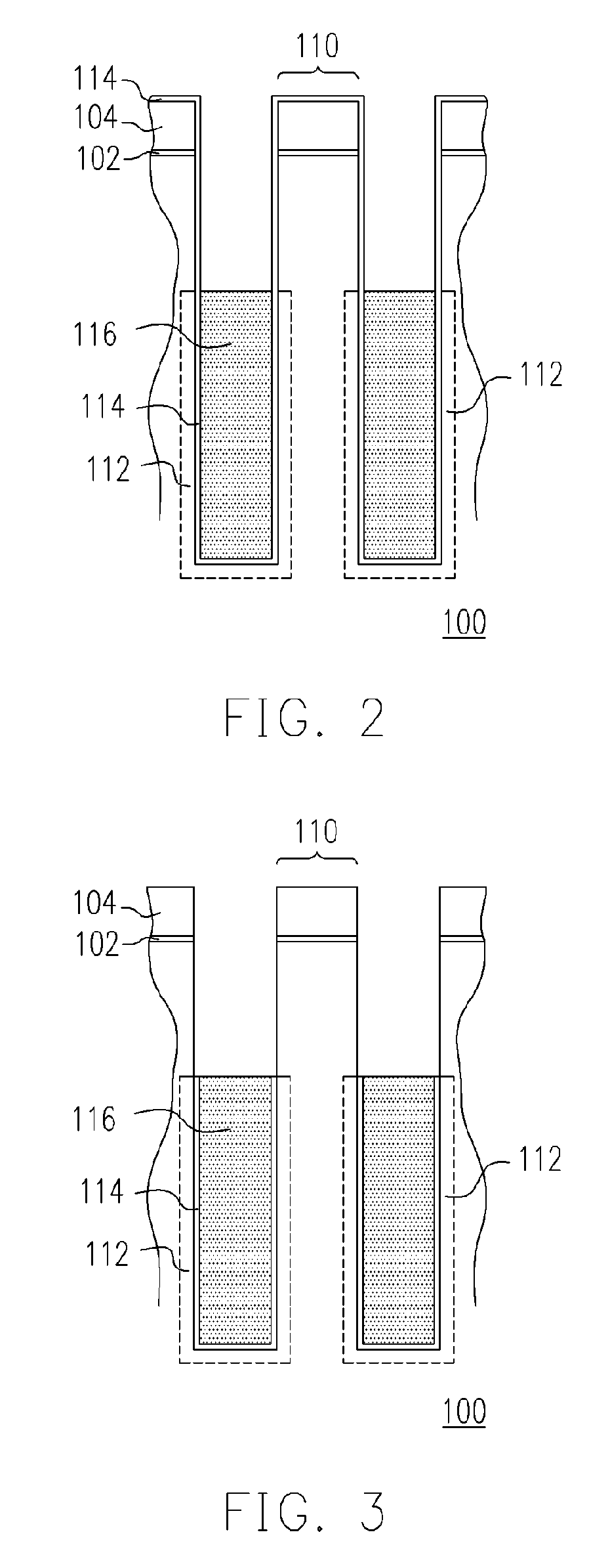
[0021]FIG. 1 clearly shows the DRAM array arrangement in a perspective view, FIGS. 2–11, 13–15 and 18(a) are cross-sectional views along line I–I′ in FIG. 1, FIG. 18(b) is another cross-sectional view, and FIGS. 12, 16 and 17 are top views.

[0022]More specifically, FIGS. 1–7 illustrate the process flow of forming the capacitors of the DRAM array, FIGS. 8–14 illustrate the process flow of forming the transistors of the DRAM array, and FIGS. 15–18 illustrate subsequent steps including the fabrications of the bit lines and the word lines.

[0023]

[0024]Referring to FIG. 1, a semiconductor substrate 100, such as a P−-doped single-crystal silicon substrate, is provided, and then a pad oxide layer 102 and a patterned mask layer 104 are formed on the substrate 100. The patterned mask layer 104 includes rows and columns of rectangular or square blocks, and is formed from an etching-resistant material like silicon nitride (SiN). The substrate 100 is etched with the patterned mask layer 104 as a ...


PUM


Abstract

A dynamic random access memory (DRAM) cell is described, including a semiconductor pillar on a substrate, a capacitor on a lower portion of a sidewall of the pillar, and a vertical transistor on an upper portion of the sidewall of the pillar. The capacitor includes a first plate in the lower portion of the sidewall of the pillar, a second plate as an upper electrode at the periphery of the first plate, a third plate at the periphery of the second plate electrically connected with the first plate to form a lower electrode, and a dielectric layer separating the second plate from the first and third plates. A DRAM array based on the DRAM cell and a method for fabricating the DRAM array are also described.

Description

CROSS-REFERENCE TO RELATED APPLICATION[0001]The present application is a continuation in-part (CIP) application of U.S. patent application of Ser. No. 10 / 605,199 filed Sep. 15, 2003, which is a CIP application of U.S. patent application of Ser. No. 10 / 210,031 filed Aug. 2, 2002 now U.S. Pat. No. 6,875,653, The entire contents thereof are incorporated herein for reference.BACKGROUND OF THE INVENTION[0002]1. Field of the Invention[0003]This invention pertains in general to semiconductor devices, and, more particularly, to cell and array structures of dynamic random access memory (DRAM) and processes for manufacturing the DRAM array. The DRAM cell features a capacitor that has a particularly high electrical capacitance.[0004]2. Description of the Related Art[0005]In the semiconductor industry, DRAM is one of the most important integrated circuits, which motivates continuing research and development. There is a continuing effort to increase the storage capacity, improve the writing and ...

Claims


Application Information

Patent Timeline
Patent Type & Authority Patents(United States)
IPC IPC(8): H01L27/108H01L29/76H01L29/94H01L31/119H01L21/336H01L21/8238H01L21/8242H01L21/8244
CPCH01L27/10832H01L27/10841H01L27/10861H01L27/10864H01L27/10867H01L27/10888H01L29/945H01L27/0207H10B12/373H10B12/395H10B12/0383H10B12/0385H10B12/038H10B12/485
Inventor WANG, TING-SHING
Owner PROMOS TECH INC
Why Eureka
Try Eureka