Single cell for fuel cell and solid oxide fuel cell
a fuel cell and single cell technology, applied in the direction of cell components, final product manufacturing, sustainable manufacturing/processing, etc., can solve the problems of loss of generation power output, achieve the effect of enhancing generation power output, compact electrolyte film, and reducing conductivity of electrolyte layer
- Summary
- Abstract
- Description
- Claims
- Application Information
AI Technical Summary
Benefits of technology
Problems solved by technology
Method used
Image
Examples
example 1
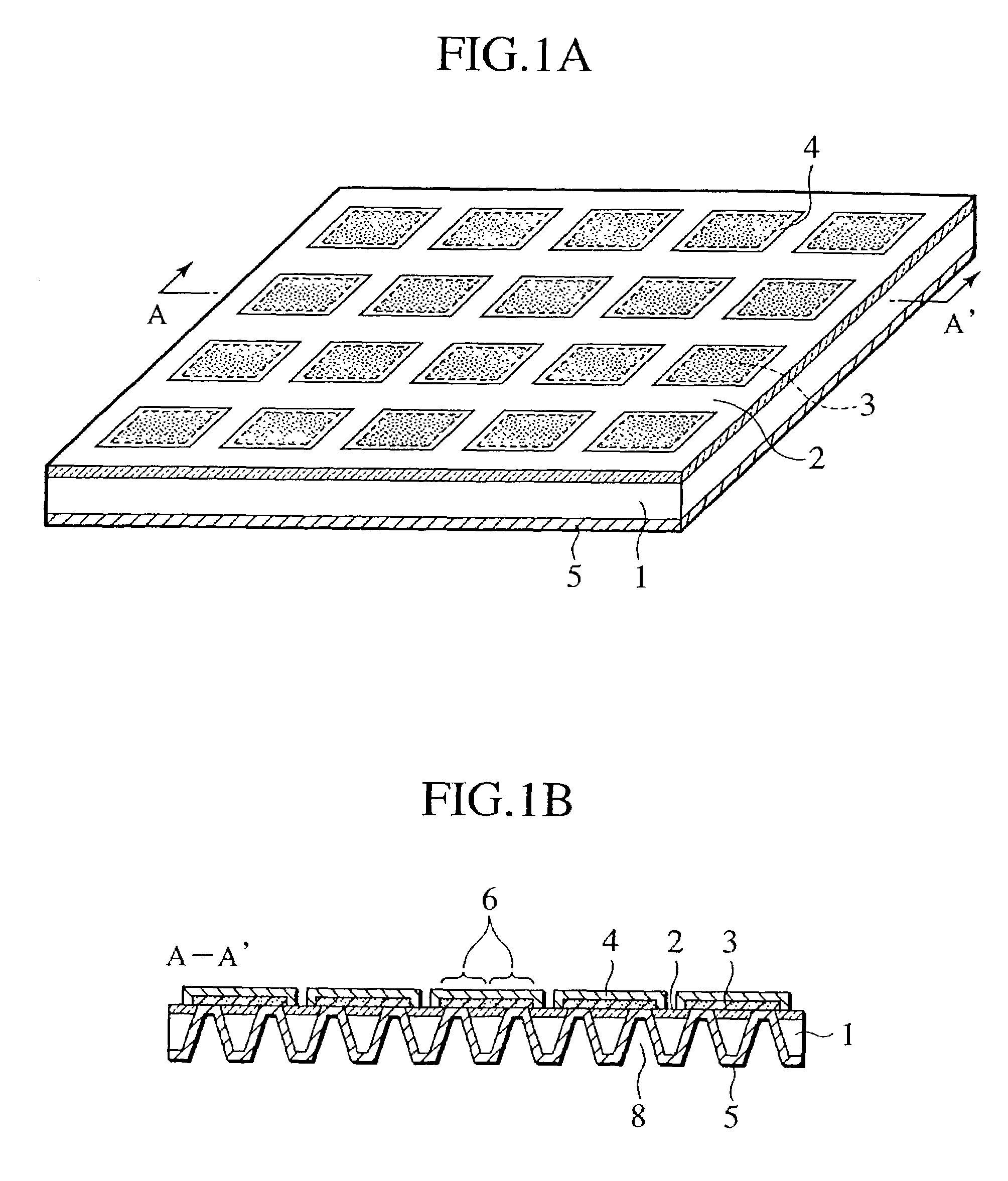
[0191]FIG. 1A is a perspective view of a cell plate of example 1, and FIG. 1B is a sectional view of this cell plate along a section line A–A′ of FIG. 1A.
[0192]10 times 10 pieces of cells 6 are formed on a Si substrate 1 of 10 cm square. Each cell 6 has a rectangular opening 8 of about 2 mm square.
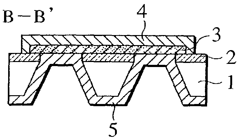
[0193]On one surface of the Si substrate 1 (hereinafter, referred to as a “upper surface”), on which a plurality of the openings 8 are formed, an insulating and stress absorbing layer 2 is formed. Moreover, on the upper surface of the substrate, on which the insulating and stress absorbing layer 2 is formed, electrolyte layers 3 and upper electrode layers 4 are formed so as to cover the openings 8. The other surface of the substrate (hereinafter, referred to as a “lower surface”) is coated with a lower electrode layer 5, and on the openings 8, the lower electrode layer 5 is exposed to the upper surface of the Si substrate 1 and directly contacts the electrolyte layers 3.
[0194]Hereinafter, ...
example 2
[0205]By use of a method similar to that in the above-described example 1, fabricated was a cell plate, on which the insulating and stress absorbing layer 2 was made of various materials. Moreover, in addition to this, also with regard to the electrolyte layer 3, cell plates of various patterns shown in FIG. 1A and FIGS. 5A to 5C were fabricated. These cell plates were placed in the electric furnace, and a heat treatment test at a temperature of 700° C. (temperature rising rate: 300° C. / Hr) in the atmosphere was executed. Results obtained are shown in a table of FIG. 6.
[0206]The pattern of FIG. 5A shows that the electrolyte layer pattern is separated for every four openings and corners of each separated pattern is chamfered. The pattern of FIG. 5B shows that an independent circular pattern is formed for every opening. The pattern of FIG. 5C shows that a continuous electrolyte layer pattern is formed on the entire surface of the cell plate.
[0207]Note that, ∘ in the table of FIG. 6 de...
example 3
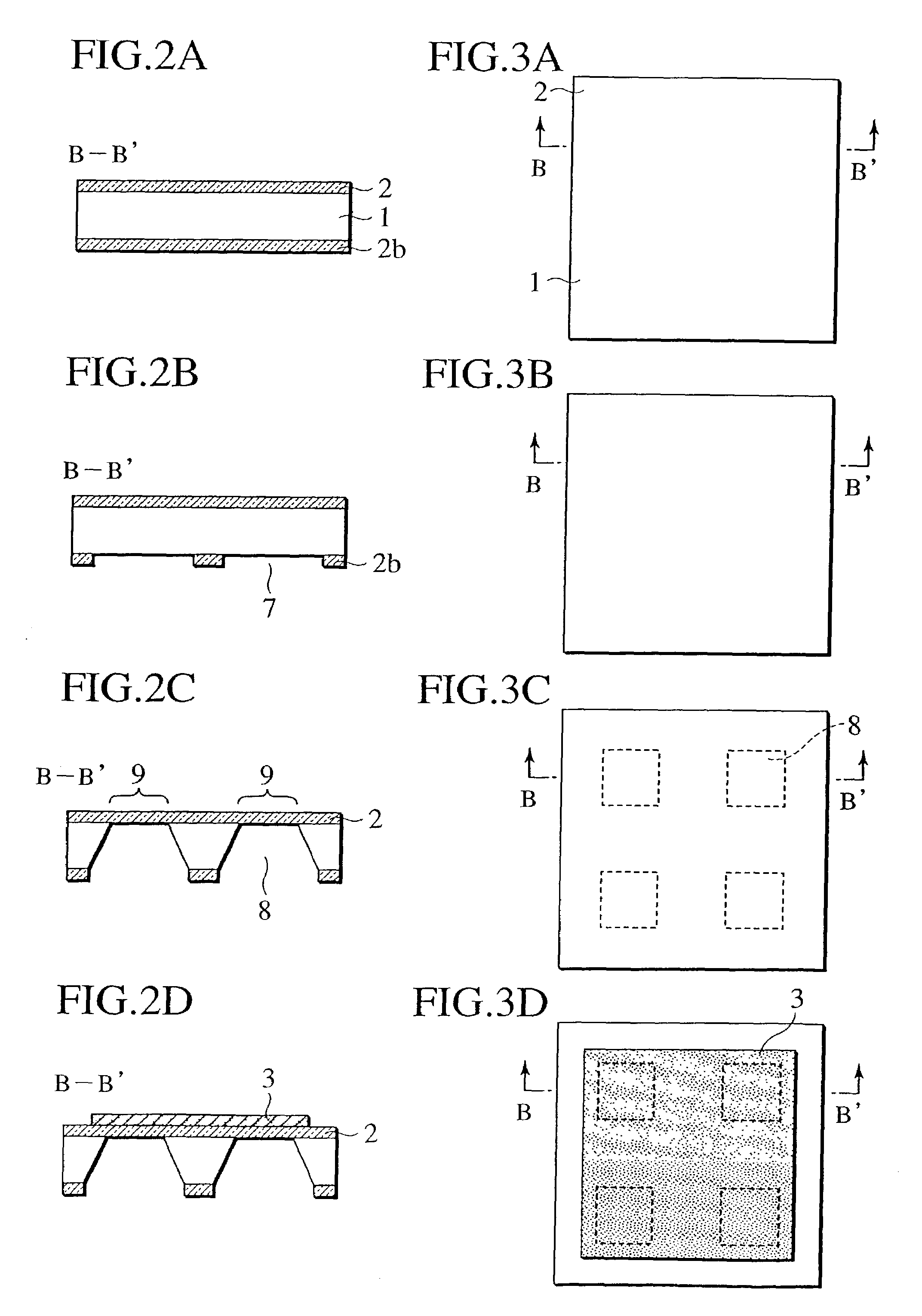
[0209]Example 3 used a Si substrate of 10 cm square similar to that of example 1, and a cell plate manufactured in accordance with manufacturing steps shown in FIGS. 7A to 7H and FIGS. 8A to 8H. FIGS. 7A to 7H are partial sectional views of the cell plate in The respective manufacturing steps, and FIGS. 8A to 8H are partial plan views of the cell plate in the respective manufacturing steps.
[0210]First, silicon nitride films as the insulating and stress absorbing layers 2 (2a) are deposited in thickness of 200 nm on the both surfaces of the Si substrate 1 by the low pressure CVD method, and a PSG layer as a reinforcement layer 12 is deposited in thickness of 100 nm on the upper surface of the substrate by a normal pressure CVD method (FIG. 7A and FIG. 8A).
[0211]Similarly to example 1, a desired region of this silicon nitride film 2a on the lower surface of the substrate is removed by the photolithography and by the chemical dry etching using CF4 gas, thus forming silicon exposure reg...
PUM
| Property | Measurement | Unit |
|---|---|---|
| thickness | aaaaa | aaaaa |
| temperature | aaaaa | aaaaa |
| thickness | aaaaa | aaaaa |
Abstract
Description
Claims
Application Information


