Semiconductor integrated circuit device

a technology of integrated circuits and semiconductors, applied in the direction of generating/distributing signals, instruments, pulse techniques, etc., can solve the problems of increasing the number of clock buffer circuits forming the cts, cts consume more current than is necessary, and the entire semiconductor integrated circuit device consumes much more current, so as to achieve the effect of reducing the input capacity of the inverter and reducing the size of the first transistor

Inactive Publication Date: 2006-10-17
RENESAS ELECTRONICS CORP
View PDF2 Cites 7 Cited by
  • Summary
  • Abstract
  • Description
  • Claims
  • Application Information

AI Technical Summary

Benefits of technology

[0011]Since the semiconductor integrated circuit device in recent years is also employed in cellular phones and mobile terminals such as a PDA, reduction in power consumption, together with faster processing are more increasingly demanded.
[0012]However, in the conventional semiconductor integrated circuit as described above, the P-channel transistor in the clock buffer circuit is formed to be larger (usually on the order of two or three times larger) than the N-channel transistor, a gate capacity of the P-channel transistor increases. An input capacity of the clock buffer circuit thus increases.
[0015]The present invention has been made to solve the problems with the conventional art, as described above. It is therefore an object of the invention to provide a semiconductor integrated circuit device that reduces charging and consumed in CTS, thereby reducing current consumption throughout entire circuits of the semiconductor integrated circuit device.
[0029]In the semiconductor integrated circuit device configured as described above, the clock buffer circuit includes the inverter: the inverter includes the first transistor that drives the load at either of the edges flank of the reference clock with which the clock synchronous type circuit does not operate in synchronization and has the gate width that has been set so that a change in the edge flank is slowed down, provided that the pulse waveform of the reference clock is not destroyed, and the second transistor that drives the load at the other edge flank of the reference clock with which the clock synchronous type circuit operates in synchronization. The type of carriers used the channel of the second transistor is different from the carrier type of the first transistor, and the second transistor is formed to have the gate width larger than the first transistor. Since a size of the first transistor thus can be more reduced than in a prior art, the input capacity of the inverter can be thereby reduced.

Problems solved by technology

A number of the clock buffer circuits that can be connected as loads is therefore restricted, resulting in an increase in the number of the clock buffer circuits constituting the CTS.
Thus, a problem has arisen that the entire semiconductor integrated circuit device consumes much more current.
Thus, a problem has arisen that the CTS consumes more current than is necessary.

Method used


Image

  • Semiconductor integrated circuit device
  • Semiconductor integrated circuit device
  • Semiconductor integrated circuit device

Examples


first embodiment

(First Embodiment)

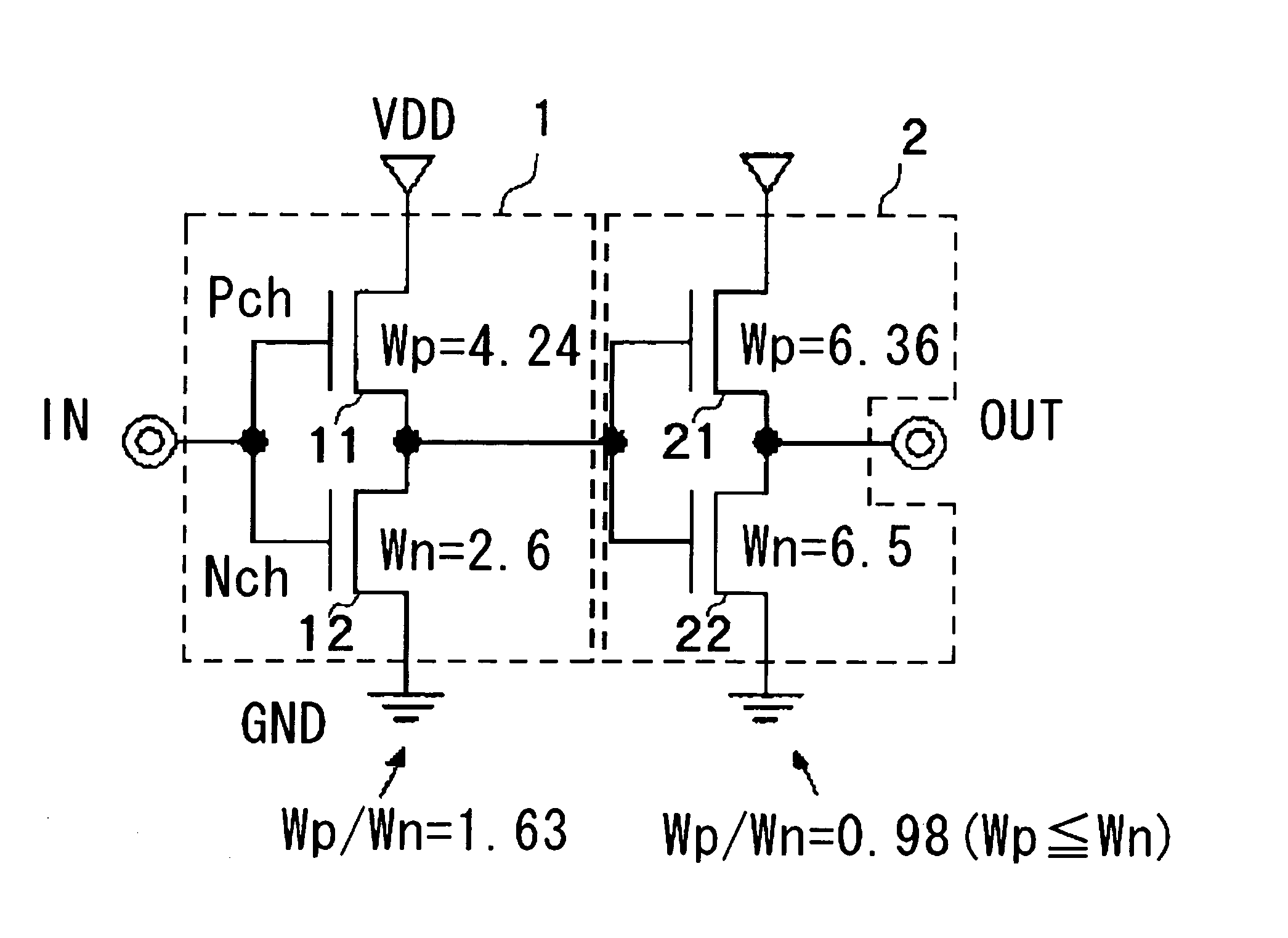
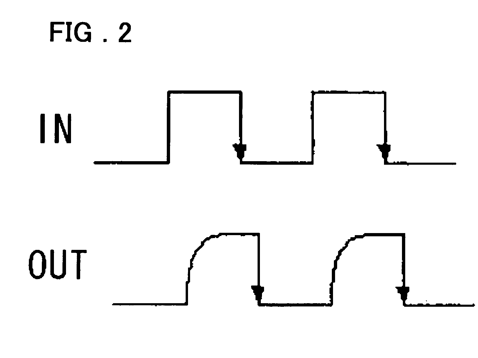
[0040]FIG. 1 is a circuit diagram showing a configuration of a clock buffer circuit provided for a semiconductor integrated circuit device according to a first embodiment of the present invention. FIG. 2 is a timing diagram showing input and output waveforms of the clock buffer circuit shown in FIG. 1. FIG. 3 is a circuit diagram showing a configuration of clock tree synthesis using the clock buffer circuit shown in FIG. 1.

[0041]The clock buffer circuit in this embodiment is configured to be applied to a clock synchronous type circuit that operates in synchronization with either of a rising edge flank or a falling edge flank of a reference clock. Each of clock buffer circuits constituting the CTS is configured to reduce its input capacity by reducing a size of a transistor for performing driving at the edge flank of the reference clock that is not used for a synchronizing operation.

[0042]As shown in FIG. 1, like a conventional clock buffer circuit, the clock buffer...

second embodiment

(Second Embodiment)

[0053]FIG. 4 is a circuit diagram showing a configuration of a clock buffer circuit provided for a semiconductor integrated 10 circuit device according to a second embodiment of the present invention. FIG. 5 is a timing diagram showing input and output waveforms of the clock buffer circuit shown in FIG. 4. FIG. 6 is a circuit diagram showing a configuration of a clock tree synthesis configuration using the clock buffer circuit shown in FIG. 4.

[0054]The clock buffer circuit in the second embodiment is configured to include a NAND gate 3 in place of the first inverter, as shown in FIG. 4.

[0055]As shown in FIG. 4, the NAND gate 3 includes a first P-channel transistor 31, a first N-channel transistor 33, a second P-channel transistor 32, and a second N-channel transistor 34. The gates of the first P-channel transistor 31 and the first N-channel transistor 33 are interconnected, and the drains of the first P-channel transistor 31 and the first N-channel transistor 33 a...


PUM


Abstract

To provide a semiconductor integrated circuit device that reduces charging and discharging currents flowing through clock tree synthesis, thereby reducing current consumption of entire circuits of the semiconductor integrated circuit device.In a semiconductor integrated circuit device including a clock synchronous type circuit that operates in synchronization with either of rising and falling edges flank of a reference clock and a plurality of clock buffer circuits for distributing the reference clock to the clock synchronous type circuit, each clock buffer circuit is constituted from a first transistor that drives a load at one of the edges flank of the reference clock with which the clock synchronous type circuit does not operate in synchronization and a second transistor that drives the load at the other edge flank of the reference clock. A gate width of the first transistor is set so that a change in the edge flank is slowed down, provided that a pulse waveform of the reference clock is not destroyed. A carrier type of the second transistor is different from the carrier type of the first transistor, and the second transistor is formed to have the gate width larger than the first transistor.

Description

FIELD OF THE INVENTION[0001]The present invention relates to a semiconductor integrated circuit device. More specifically, the invention relates to the semiconductor integrated circuit device having a clock synchronous type circuit that operates in synchronization with either of a rising edge flank or a falling edge flank of a reference clock.BACKGROUND OF THE INVENTION[0002]When the clock synchronous type circuit including a plurality of flip-flops (that will be referred below as F / Fs) that operate in synchronization with the reference clock is formed in the semiconductor integrated circuit device such as an ASIC (Application Specific Integrated Circuit), the reference clock is supplied to each of the F / Fs using a plurality of clock buffer circuits for distributing the reference clock.[0003]FIG. 7 is a circuit diagram showing a conventional clock buffer circuit provided for a semiconductor integrated circuit device, and FIG. 8 is a timing diagram showing input and output waveforms ...

Claims


Application Information

Patent Timeline
Patent Type & Authority Patents(United States)
IPC IPC(8): H01L29/72H01L21/822G06F1/12G11C11/41H01L21/82H01L27/04H01L29/76H03K5/15H03K17/16H03K17/687H03K19/0175
CPCG06F1/12H03K5/1506F24F12/001F24F13/28F24F2012/008
Inventor HONDA, TAKAO
Owner RENESAS ELECTRONICS CORP
Why Eureka
Try Eureka