

Chemical vapor deposition chamber pre-deposition treatment for improved carbon doped oxide thickness uniformity and throughput
- Summary
- Abstract
- Description
- Claims
- Application Information
AI Technical Summary
Benefits of technology
Problems solved by technology
Method used
Image

Examples
Embodiment Construction
[0013]In the following detailed description, numerous specific details are set forth in order to provide a thorough understanding of the invention. However, it will be understood by those skilled in the art that the present invention may be practiced without these specific details. In other instances, well-known methods, procedures, components and circuits have not been described in detail so as not to obscure the present invention.
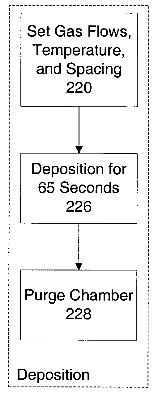
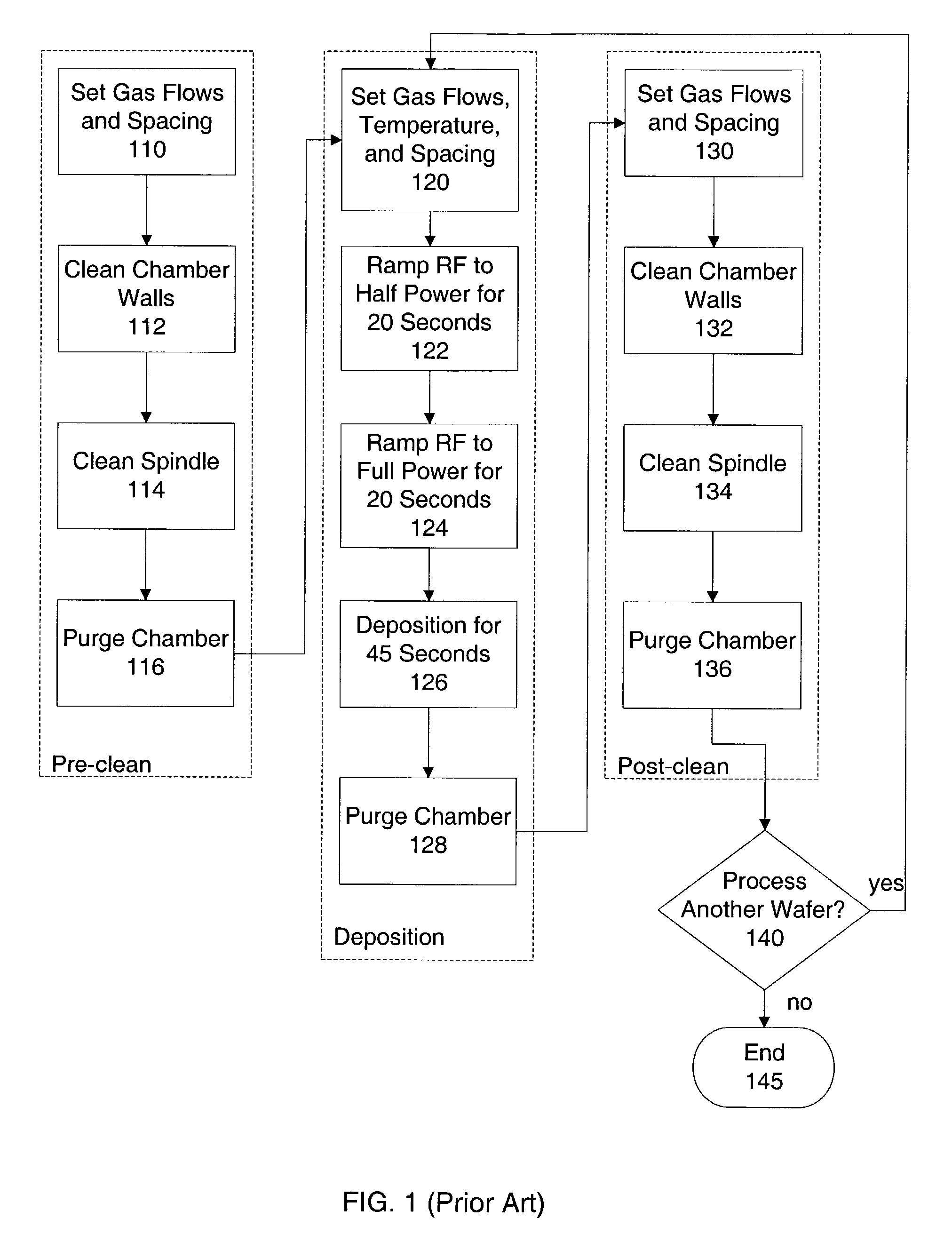
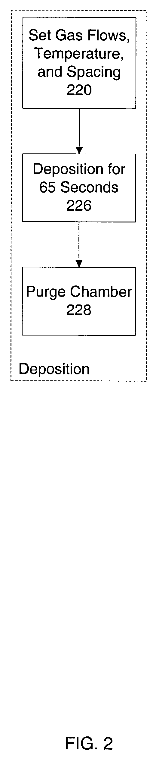
[0014]For one embodiment of the invention, pre-deposition operations 122 and 124 of FIG. 1 are eliminated to improve processing throughput. As stated above, operations 122 and 124 take up approximately 20 seconds each. Thus, eliminating operations 122 and 124 reduces processing time by 40 seconds if the same dielectric quality can be achieved. Without pre-deposition operations 122 and 124, however, experiments show that the deposition time of operation 126 needs to be increased by approximately 20 seconds to achieve the same dielectric thickness.
[0015]FIG...
PUM
| Property | Measurement | Unit |
|---|---|---|
| Time | aaaaa | aaaaa |
| Thickness | aaaaa | aaaaa |
| Pressure | aaaaa | aaaaa |
Abstract
Description
Claims
Application Information