Power supply, a semiconductor making apparatus and a semiconductor wafer fabricating method using the same

a technology of semiconductor wafers and fabrication methods, applied in the field of power supplies, can solve the problems of large amount of money lost, system failure to detect any fault during the semiconductor wafer fabrication, and increase so as to achieve the effect of increasing the diameter the value added of the semiconductor wafer today, and increasing the potential loss due to defects in lot units

Active Publication Date: 2006-10-24
HITACHI HIGH-TECH CORP
View PDF5 Cites 1 Cited by
  • Summary
  • Abstract
  • Description
  • Claims
  • Application Information

AI Technical Summary

Benefits of technology

[0008]As a result, although the operation is achieved according to the predetermined setting value, the system cannot detect any fault during the semiconductor wafer fabrication. Until a defect of a semiconductor wafer thus processed is detected in a process downstream the fabrication process, the semiconductor wafers with the defect are continuously fabricated in each lot unit including, for example, 25 semiconductor wafers. This possibly leads to loss of a large amount of money. The diameter of the semiconductor wafer and the value added to the semiconductor wafer are increasing today. Therefore, potential of the loss due to defects in lot unit is increasing. In the field of semiconductor making apparatuses, a need exists for higher precision of the output power from these power supplies. This reduces the allowed range of only explicit abnormalities of constituent components but also a fine offset value due to gradual aging or the like. It is therefore important to detect occurrence of a fine offset to prevent defects.

Problems solved by technology

However, the control microcomputer 1 cannot detect occurrence of the abnormal offset and hence determines that the situation is normal.
As a result, although the operation is achieved according to the predetermined setting value, the system cannot detect any fault during the semiconductor wafer fabrication.
This possibly leads to loss of a large amount of money.
Therefore, potential of the loss due to defects in lot unit is increasing.
This reduces the allowed range of only explicit abnormalities of constituent components but also a fine offset value due to gradual aging or the like.

Method used


Image

  • Power supply, a semiconductor making apparatus and a semiconductor wafer fabricating method using the same
  • Power supply, a semiconductor making apparatus and a semiconductor wafer fabricating method using the same
  • Power supply, a semiconductor making apparatus and a semiconductor wafer fabricating method using the same

Examples


first embodiment

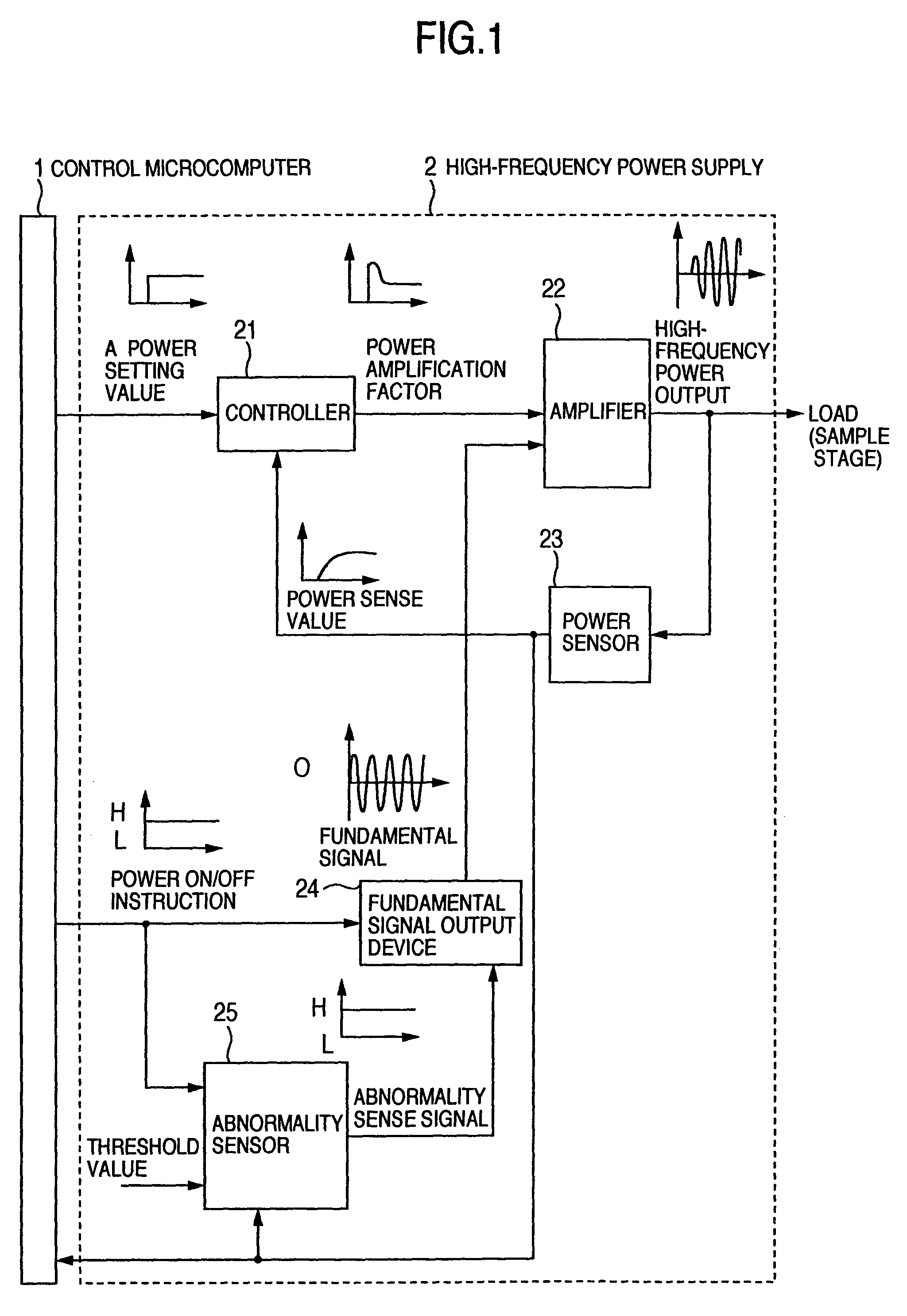
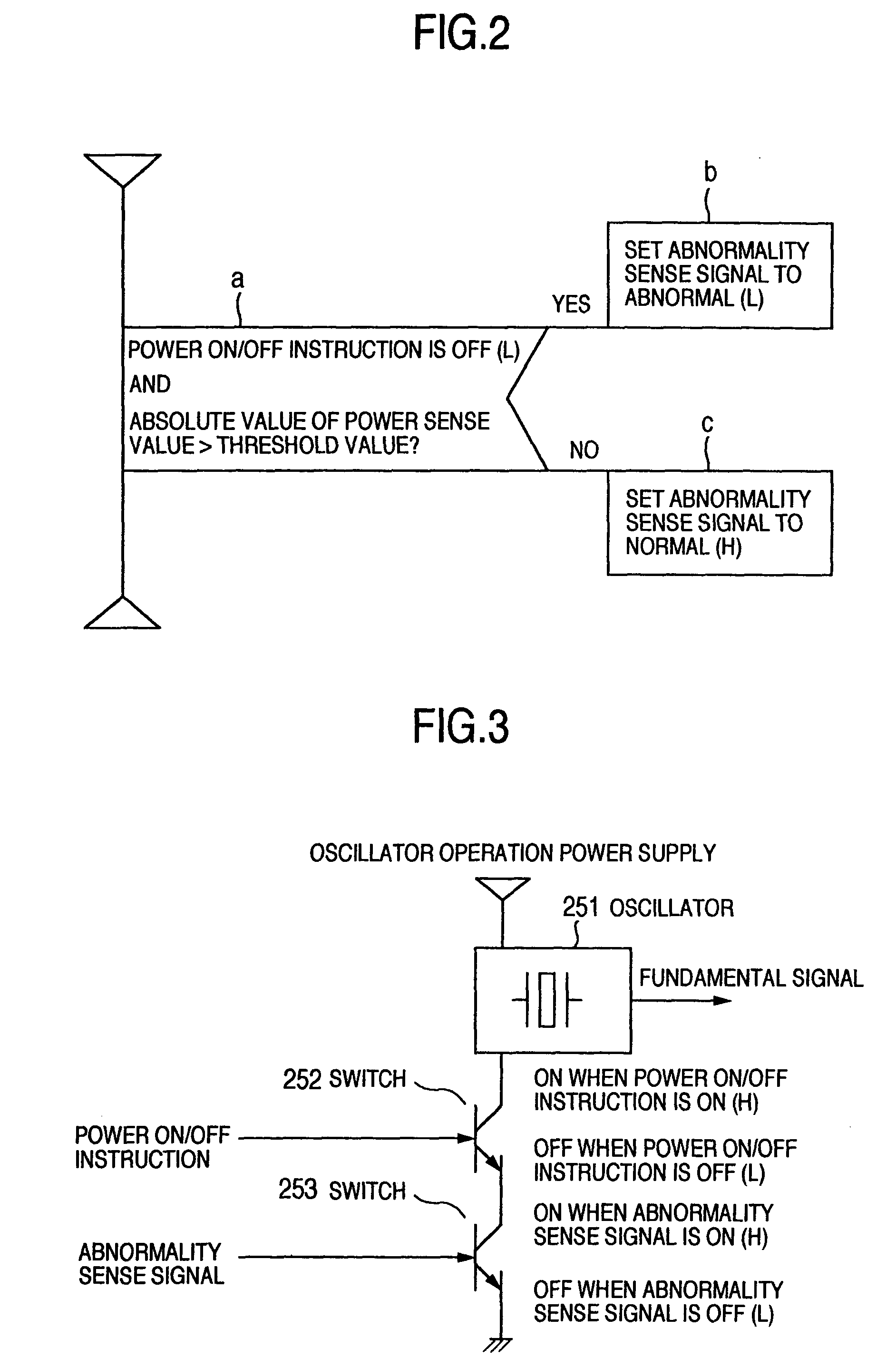
[0022]Description will now be given of the present invention by referring to the drawings. FIG. 1 shows an embodiment of the present invention. In FIG. 1, the embodiment includes high-frequency power supply 2 for a semiconductor making apparatus. The power supply 2 includes a controller 21, an amplifier 22, a power sensor 23, a fundamental signal output device 24, and an abnormality sensor 25. The power sensor 23 senses strength of power produced from the power supply 2 and outputs a power sense signal according to the strength. The abnormality sensor 25 receives a power on / off instruction to instruct whether or not power is to be outputted, the power sense signal, and a predetermined threshold value, determines whether or not an abnormal offset occurs in the power sense value, and outputs an abnormality sense signal indicating a result of the determination. The fundamental signal output device 24 receives the power on / off instruction and the abnormality sense signal to output a fun...

second embodiment

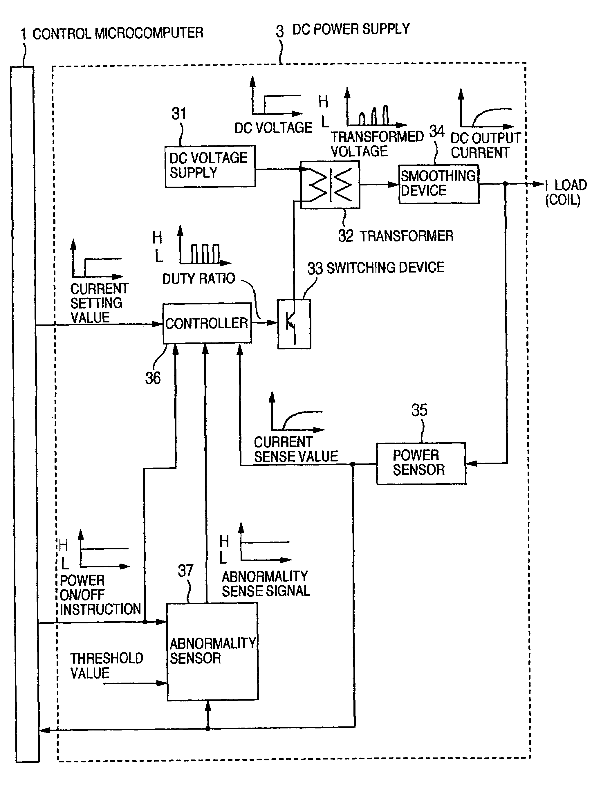
[0042]Description will now be given of the present invention by referring to the drawings. In FIG. 4, dc power supply 3 for a semiconductor making apparatus outputs a dc current such that a coil as a load generates a desired magnetic field. The dc power supply includes a dc voltage device 31, a voltage transformer 32, a switching device 33, a smoothing device 34, a current sensor 35, a controller 36, and an abnormality sensor 37. The current sensor 35 senses strength of a current outputted from the dc power supply to output a current sense signal according to the strength. The abnormality sensor 37 receives a power on / off instruction to instruct whether or not a current is to be outputted, the current sense signal, and a predetermined threshold value, determines whether or not an abnormal offset occurs in the current sense value, and outputs an abnormality sense signal indicating a result of the determination. The controller 36 outputs a duty ratio according to the power on / off inst...


PUM


Abstract

In power supply and a semiconductor making apparatus and a semiconductor fabricating method using the same, an abnormality can be detected when an offset occurs in a part constituting a closed-loop system of high-frequency power supply or dc power supply for a semiconductor making apparatus. Power supply for receiving a power value setting signal to set strength of power and a power on/off instruction to set on or off of outputting of the power interrupts the supply of the power even in a state in which a subsequent power on/off instruction is on if a power sense signal according to a value obtained by sensing the power exceeds a predetermined value when the power on/off instruction is off.

Description

CROSS-REFERENCE TO RELATED APPLICATIONS[0001]This application is a division of application Ser. No. 10 / 082,160 filed on Feb. 26, 2002 now U.S. Pat. No. 6,713,885. The contents of application Ser. No. 10 / 082,160 are hereby incorporated herein by reference in their entirety.BACKGROUND OF THE INVENTION[0002]The present invention relates to power supply, and in particular, to power supply to process a semiconductor wafer and a semiconductor making apparatus and a semiconductor fabricating method using the same.[0003]Etching systems using plasma have been used in various fields and include an electron cyclotron resonance (ECR) etching system. In the ECR etching system, by applying a direct current (dc) flows to a coil disposed on an outer surface of a vacuum chamber or container, a magnetic field is generated, and a high voltage is applied to a magnetron to start oscillation. This introduces a microwave into the vacuum chamber to resultantly generate plasma therein. Ions incident to a sa...

Claims


Application Information

Patent Timeline
Patent Type & Authority Patents(United States)
IPC IPC(8): H01L21/66G01R31/40G05F1/10H01J37/32
CPCG01R31/40H01J37/32082H01J37/32174
Inventor TAKAHASHI, YOUJIIIDA, TSUTOMUUMEMOTO, TSUYOSHIKASHIBE, MAKOTO
Owner HITACHI HIGH-TECH CORP
Why Eureka
Try Eureka