Increased light extraction from a nitride LED

a technology of led chips and nitride, which is applied in the field of electronic arts, can solve the problems of high cost, significant degradation of the light output power of the led chip, and optical reflective loss at the interface between the substrate and the epitaxial layer,

Inactive Publication Date: 2006-10-24
GELCORE LLC (US)
View PDF32 Cites 70 Cited by
  • Summary
  • Abstract
  • Description
  • Claims
  • Application Information

AI Technical Summary

Benefits of technology

[0008]In accordance with another aspect of the present application, a lateral current flip-chip light emitting diode device with a removed growth substrate is provided. The light emitting diode device includes a mount including bonding pads. A die active side is bonded to bonding bumps of the mount to securely fasten the active side to the mount. An underfill material is arranged between the active side and the mount. The underfill material supports the die and prevents the die from fracturing. A plurality of irregularities is formed on an exposed top surface of the layers stack defining a roughened top surface which improves light extraction by scattering the emitted light outward.

Problems solved by technology

A problem can arise in the flip-chip configuration when the growth substrate is substantially light-absorbing over some or all of the spectral range of light emission.
Moreover, even if a suitable optically transparent substrate is available, such as is the case for group III-nitride light emitting diodes which can be grown on transparent sapphire, optical reflective losses can occur at the interface between the substrate and the epitaxial layers due to an abrupt discontinuity in refractive index.
As a result, while the removal of the sapphire substrate from a nitride-based flip chip provides the above benefit, it also causes a significant degradation of the light output power of the LED chip.
However, dry etching has a possibility of damaging the chip and involves high costs.
The problem with wet etching is that GaN is not easily etched by most solutions and if it can be etched, the etch rate is too slow for effective processing.
However, photoelectrochemical etching requires a complex setup to provide an electric potential over the surface being etched and deposit metal on GaN film that serves as an electrical contact.

Method used


Image

  • Increased light extraction from a nitride LED
  • Increased light extraction from a nitride LED
  • Increased light extraction from a nitride LED

Examples


Embodiment Construction

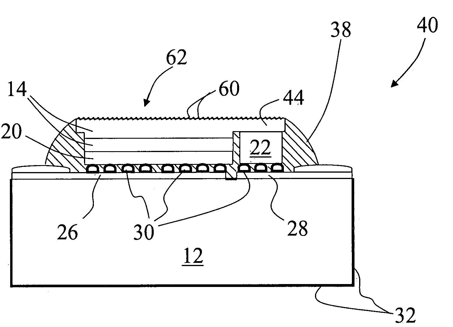
[0015]With reference to FIG. 1, a light emitting die 10 is mounted in flip-chip fashion on a mount or submount wafer 12. The die 10 includes a semiconductor device layers stack 14 that is epitaxially deposited on a growth substrate 16. The epitaxial device layers stack 14 can comprise a group III nitride ultraviolet or blue light material, a group III phosphide visible-emission material, or the like.

[0016]The semiconductor layers stack 14 is depicted with two exemplary layers corresponding to a simple p / n diode; however, those skilled in the art will appreciate that more complex semiconductor layer stack can be employed. For a group III nitride ultraviolet or blue light emitting diode with a p-on-n orientation, the layers stack typically includes an epitaxial growth buffer of aluminum nitride or another material, an n-type gallium nitride base layer, an active region of indium gallium nitride, a p-type gallium nitride layer, and optionally a contact layer formed on the p-type galliu...


PUM


Abstract

In a method for fabricating a flip-chip light emitting diode device, a submount wafer is populated with a plurality of the light emitting diode dies. Each device die is flip-chip bonded to the submount. Subsequent to the flip-chip bonding, a growth substrate is removed. The entire submount is immersed in the etchant solution, exposed to the light for a prespecified period of time, removed from the solution, dried and diced into a plurality of LEDs. The LEDs are immediately packaged without any further processing.

Description

BACKGROUND[0001]The present application relates to the electronics arts. It particularly relates to group III-nitride flip-chip bonded light emitting diodes for lighting applications, and will be described with specific reference thereto. However, it also finds application in conjunction with other types of flip-chip bonded epitaxial semiconductor devices, and the like.[0002]In a flip-chip mounting configuration, a light emitting diode with a light-transmissive substrate and front-side electrodes is bonded “face down” to bonding bumps of a mount, that is, with the epitaxial layers proximate to the mount and a light-transmissive substrate distal from the mount. The flip-chip arrangement has a number of advantages, including improved thermal heat sinking due to the proximity of the active layers to the submount, and reduction of electrode shadowing losses.[0003]In the flip-chip mounting configuration, light is extracted from the substrate side. For epitaxially grown light emitting dio...

Claims


Application Information

Patent Timeline
Patent Type & Authority Patents(United States)
IPC IPC(8): H01L21/00H01L33/00H01L33/22H01L33/62
CPCH01L33/22H01L33/0079H01L33/62H01L2224/16H01L2924/00014H01L33/0093H01L2224/05644H01L2224/05599H01L2224/0555H01L2224/0556H01L2224/05568H01L2224/05573H01L2224/0554
Inventor SACKRISON, MICHAEL J.VENUGOPALAN, HARI S.GAO, XIANG
Owner GELCORE LLC (US)
Why Eureka
Try Eureka