Method for removing impurities of a semiconductor wafer, semiconductor wafer assembly, and semiconductor device

Inactive Publication Date: 2006-10-24
HYOGO PREFECTURAL GOVERNMENT
View PDF7 Cites 0 Cited by
  • Summary
  • Abstract
  • Description
  • Claims
  • Application Information

AI Technical Summary

Benefits of technology

[0019]According to the present invention, since the impurities-removing region is directly provided on the semiconductor wafer to perform the gettering treatment for the impurities of the surface region of the semiconductor wafer by the impurities-removing region, the impurities can be removed effectively and efficiently, compared with conventional techniques such as a gettering treatment utilizing a polycrystalline silicon film or an intrinsic gettering treatment utilizing minute defects. For example, since the impurities-removing region is directly formed on the SOI wafer, the impurities of the surface thin silicon layer of the SOI wafer can be removed effectively and efficiently without the impediment of the BOX layer formed in the SOI wafer.
[0020]Therefore, if a semiconductor device is made of the semiconductor wafer from which impurities are removed on the above-mentioned technique, a satisfactory p-n junction can be made in the semiconductor device and thus, the performance of the semiconductor device can not be almost deteriorated.
[0021]In a preferred embodiment of the present invention, the impurities-removing region is provided so as to include an insulating region which insulates a semiconductor device-forming region electrically of the semiconductor wafer. In this case, since the semiconductor-forming region is not narrowed and contaminated by the impurities-removing region, the subsequent semiconductor device fabricating process can not be affected by the semiconductor device-forming region. Therefore, the product yield and the performance of the semiconductor device can not be almost deteriorated.
[0023]In still another preferred embodiment, the gettering treatment is performed while the semiconductor wafer is heated to 400° C. or over. In this case, the impurities are activated by the thermal energy and thus, diffused rapidly, so that the impurities can be removed more effectively and efficiently from the semiconductor wafer.

Problems solved by technology

In a semiconductor device made of a semiconductor wafer and various semiconductor components formed on the semiconductor wafer, it was important problem to remove heavy metal impurities of a semiconductor device during the fabricating process because the performance of the semiconductor device is deteriorated if the heavy metal impurities are incorporated in the semiconductor device even in minute amount.
If the heavy metal impurities are incorporated in the semiconductor device to deteriorate the performance thereof, the product yield of IC circuit or LSI circuit composed of many integrated semiconductor devices is decreased conspicuously and thus, the IC circuits or the LSI circuits can not be fabricated profitably.
With the SOI wafer with the BOX layer, it is difficult to remove the harmful heavy metal impurities of the thin silicon layer 12 due to the BOX layer 11 because the diffusion velocities of the heavy metal impurities such as iron and nickel in an oxide film are very small and thus, the heavy metal impurities can not be removed through the BOX layer as an oxide layer by the Gettering treatment.

Method used


Image

  • Method for removing impurities of a semiconductor wafer, semiconductor wafer assembly, and semiconductor device
  • Method for removing impurities of a semiconductor wafer, semiconductor wafer assembly, and semiconductor device
  • Method for removing impurities of a semiconductor wafer, semiconductor wafer assembly, and semiconductor device

Examples


Embodiment Construction

[0045]This invention will be described in detail hereinafter.

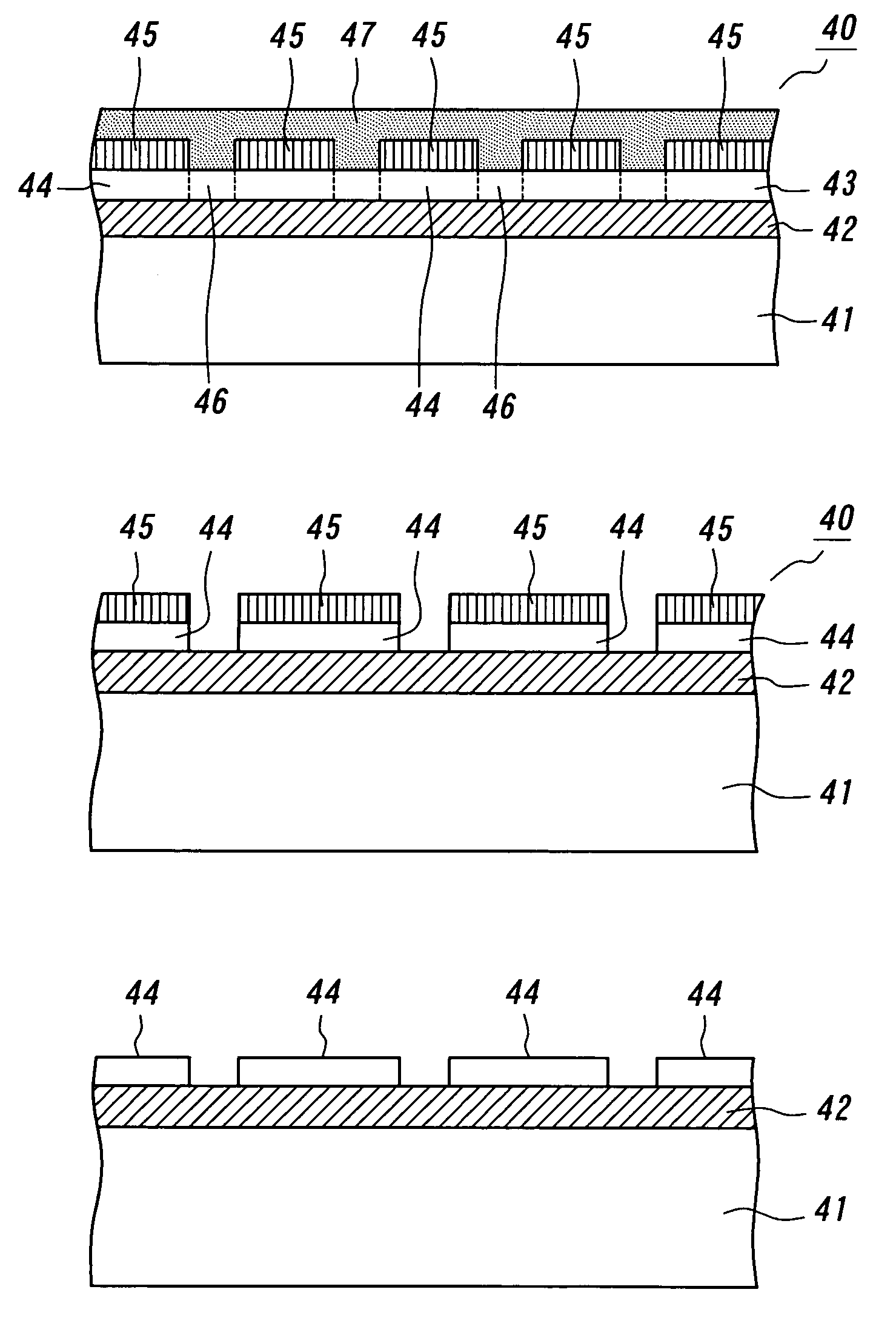
[0046]FIGS. 7–12 relate to an impurities-removing method according to the present invention. FIGS. 7, 9 and 11 are top plan views showing a semiconductor wafer under operation, and FIGS. 8, 10 and 12 are cross sectional views of the semiconductor wafer, taken on line “I—I”. In this embodiment, the impurities-removing method will be carried out for an SOI wafer.

[0047]First of all, as shown in FIGS. 7 and 8, an insulating layer 32 made of SiO2 or the like and a silicon layer 33 are formed on a silicon substrate 31 to form an SOI wafer 30. Then, on the silicon layer 33 is defined a semiconductor device-forming region 34 to form semiconductor devices and an insulating region 36 to electrically insulate the semiconductor device-forming region 34.

[0048]Then, as shown in FIGS. 9 and 10, mechanical distortion is imparted only to the insulating region 36 to form a distorted layer 38 as an impurities-removing region. Since much latt...


PUM


Abstract

On a silicon layer of an SOI wafer is defined a semiconductor device-forming region to form semiconductor devices thereon and an insulating region to electrically insulate the semiconductor device-forming region. Then, a mask layer is formed of nitride by means of photolithography so as to cover the semiconductor device-forming region. Then, an impurities-removing layer is formed by means of well known technique so as to cover the mask layer and embed the gaps between the adjacent masks of the mask layer. The impurities of the silicon layer of the SOI wafer are absorbed and removed by the distorted layer, the grain boundaries and the lattice defects of the impurities-removing layer.

Description

BACKGROUND OF THE INVENTION[0001]1. Field of the Invention[0002]This invention relates to a method for removing impurities of a semiconductor wafer such as a silicon wafer or a SOI wafer, and to a semiconductor wafer assembly which is made during the removing process of the impurities of the semiconductor wafer. This invention also relates to a semiconductor device utilizing the semiconductor wafer cleaned in impurities by the above removing method.[0003]2. Description of the Related Art[0004]In a semiconductor device made of a semiconductor wafer and various semiconductor components formed on the semiconductor wafer, it was important problem to remove heavy metal impurities of a semiconductor device during the fabricating process because the performance of the semiconductor device is deteriorated if the heavy metal impurities are incorporated in the semiconductor device even in minute amount.[0005]If the heavy metal impurities are incorporated in the semiconductor device to deterio...

Claims


Application Information

Patent Timeline
IPC IPC(8): H01L27/12H01L21/322H01L21/762H01L23/26
CPCH01L21/3226H01L21/7624H01L23/26Y10S257/913H01L2924/0002H01L2924/00
Inventor KISHINO, SEIGOTSUYA, HIDEKI
Owner HYOGO PREFECTURAL GOVERNMENT
Why Eureka
Try Eureka