Circuit board, method of producing same, and power module

a technology of circuit boards and power modules, applied in the field of circuit boards, method of producing same, and power modules, can solve the problems of ceramic substrates that may develop cracks, long-term reliability tends to be unsatisfactory, and crystals within the conductive layer growing overly larg

Inactive Publication Date: 2006-10-31
MITSUBISHI MATERIALS CORP
View PDF21 Cites 27 Cited by
  • Summary
  • Abstract
  • Description
  • Claims
  • Application Information

AI Technical Summary

Benefits of technology

[0012]The conductive layers may use a rolled material comprising 20 ppm or more of each of Cu, Fe and Si. The conductive layers may be rolled with a draft of at least 15%. In such cases, abnormal growth of the Al crystals can be suppressed, enabling a reduction in the variation of the crystal grain diameter.
[0013]The surface area of the crystal with the maximum crystal grain diameter preferably accounts for no more than 15% of the surface area of the insulating ceramic substrate. In such cases, the effect of the present invention in preventing anisotropy of the mechanical characteristics of the conductive layers is particularly strong.
[0014]The insulating ceramic substrate may be formed from at least one of Al2O3, AlN and Si3N4. The conductive layers may be bonded to the insulating ceramic substrate using a brazing material. The brazing material may be one or more materials selected from a group consisting of Al—Si based materials, Al—Ge based materials, Al—Mn based materials, Al—Cu based materials, Al—Mg based materials, Al—Si—Mg based materials, Al—Cu—Mn based materials, and Al—Cu—Mg—Mn based materials. In such cases, the bonding between the conductive layers and the insulating ceramic substrate is favorable.
[0017]The above production method may comprise an additional step for producing the conductive layer by heat treating a plate material comprising at least 99.98% by mass of aluminum, and then conducting rolling with a draft of at least 15%. By ensuring a draft of at least 15% from the final heat treatment, the 0.2% proof stress value of the conductive layer can be set at no more than approximately 35 N / mm2, and the Al material work hardening coefficient can be set at no more than approximately 0.18. As a result, the effect of the present invention in preventing cracking of the ceramic substrate on exposure to repeated temperature variations can be further strengthened. For example, if a −40° C. to 125° C. temperature cycle test is conducted, then the number of cycles before cracking develops in the substrate can be increased. A temperature cycle test is a test in which a temperature treatment, in which a single cycle involves, for example, holding the circuit board at −40° C. for 30 minutes and then at 125° C. for 30 minutes in a thermal shock tester, is carried out repeatedly.
[0018]According to the present invention, because the average crystal grain diameter of the conductive layer is kept within a range from 0.5 mm to 5 mm, and the standard deviation σ of the crystal grain diameter is no more than 2 mm, anisotropy is unlikely to develop in the mechanical characteristics of the conductive layer, enabling a reduction in the occurrence of warping of the circuit board. Furthermore, because the conductive layer comprises at least 99.98% by mass of aluminum, the stress alleviating capabilities of the layer are good, and cracking of the ceramic substrate is unlikely even when exposed to temperature variation. Accordingly, the present invention enables not only a reduction in the warping of the circuit board, but also enables prevention of other problems such as cracking of the ceramic substrate on exposure to temperature variation.
[0020]The average crystal grain diameter of the conductive layer is even more preferably within a range from 0.8 mm to 1.5 mm, and the standard deviation a of the crystal grain diameter is even more preferably 1 mm or smaller. In such cases, problems such as cracking of the ceramic substrate on exposure to temperature variation can be even more reliably prevented.

Problems solved by technology

In those cases where the conductive layer and the heat radiating plate are Cu, the generation of thermal stress caused by the differing levels of thermal expansion of the ceramic substrate and the solder is unavoidable, and as a result, the long term reliability tends to be unsatisfactory.
In such cases, following the brazing process, warping can develop when the structure is returned to normal temperatures, and this warping can cause problems in the circuit board production process and the assembly process used for producing power modules.
As shown in FIG. 3A, it is thought that the cause of this warping is the Al crystals within the conductive layer growing overly large during the brazing process.
If the crystal grain diameter becomes overly large, then anisotropy develops in the mechanical characteristics of the conductive layers formed on both surfaces of the insulating ceramic substrate, and the resulting unbalanced stresses cause warping.
As a result, if the 0.2% proof stress value or the work hardening coefficient of the Al exceed certain reference values, then when, for example, −40° C. to 125° C. temperature cycle testing is conducted, the ceramic substrate may develop cracking.

Method used


Image

  • Circuit board, method of producing same, and power module
  • Circuit board, method of producing same, and power module
  • Circuit board, method of producing same, and power module

Examples


example 1

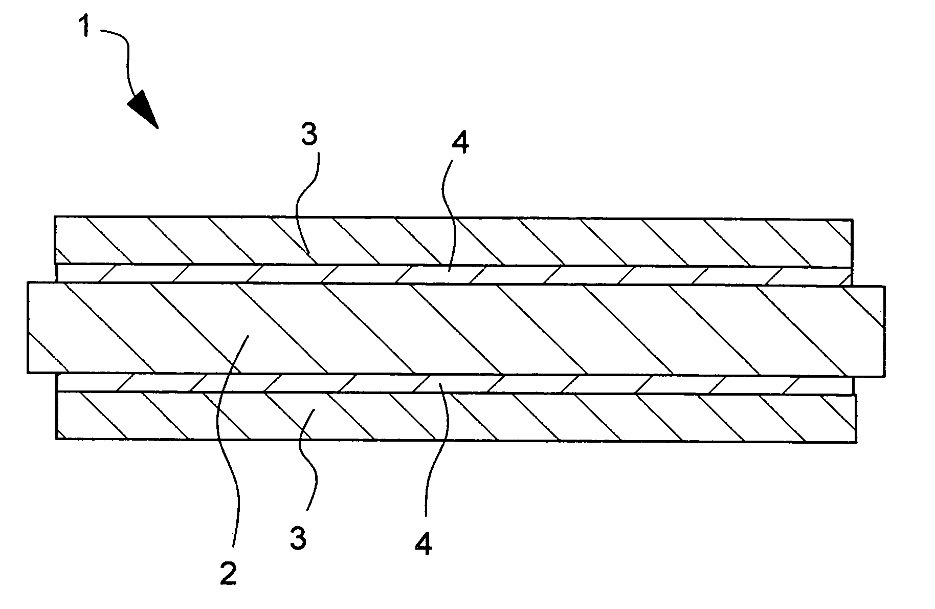
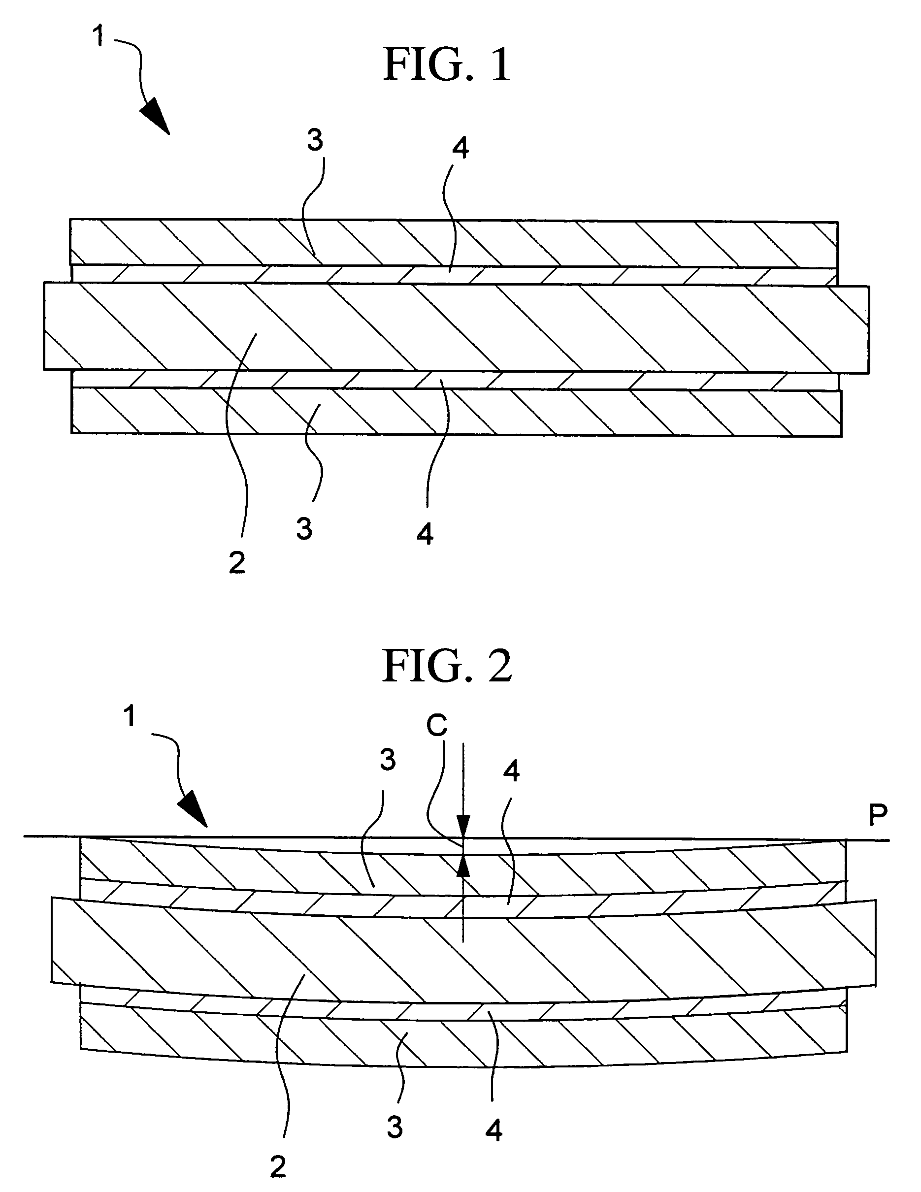
[0058]A power module of the structure shown in FIG. 4 was prepared.

[0059]On both surfaces of an AlN ceramic substrate 2 of dimensions 50 mm×50 mm×0.635 mm were bonded Al plates 3 with the same length and width dimensions as the insulating ceramic substrate 2 but with a thickness of 0.4 mm, thus preparing a circuit board 1. The Al plates 3 were prepared by a final heat treatment at 450° C., followed by rolling with a draft of 30%, and comprised 99.99% by mass of Al, as well as 23 ppm of Cu, 30 ppm of Si, and 33 ppm of Fe. The brazing material 4 used an Al—Si based brazing material comprising 8% by mass of Si. The melting point of this brazing material was 626° C. With an Al plate 3, a sheet of the Al—Si based brazing material 4, the insulating ceramic substrate 2, another sheet of the Al—Si based brazing material 4, and another Al plate 3 overlaid on top of one another, in that order, the layers were bonded together by subjecting the layered structure to a pressure of 200 kPa, heatin...


PUM

PropertyMeasurementUnit
crystal grain diameteraaaaaaaaaa
temperatureaaaaaaaaaa

Abstract

A circuit board including conductive layers bonded to both surfaces of an insulating ceramic substrate, with a brazing material disposed therebetween. The conductive layers comprise at least 99.98% by mass of aluminum, and display an average crystal grain diameter within a range from 0.5 mm to 5 mm and a standard deviation σ for that crystal grain diameter of no more than 2 mm. Each conductive layer comprises at least 20 ppm of Cu, Fe and Si. The surface area of the crystal with the maximum crystal grain diameter within the conductive layers accounts for no more than 15% of the surface area of the insulating ceramic substrate.

Description

CROSS-REFERENCE TO PRIOR APPLICATION[0001]This is a U.S. national phase application under 35 U.S.C. §371 of International Patent Application No. PCT / JP03 / 05054 filed Apr. 21, 2003, and claims the benefit of Japanese Patent Application Nos. 2002-118359 filed Apr. 19, 2002 and 2003-88129 filed Mar. 27, 2003 which are incorporated by reference herein. The International Application was published in Japanese on Oct. 30, 2003 as WO 03 / 090277 A1 under PCT Article 21(2).TECHNICAL FIELD[0002]The present invention relates to a power module, as well as a circuit board used in a power module, and a method of producing the circuit board. This technology is particularly applicable to the power modules for high-reliability inverters used in HEV (Hybrid Electric Vehicles) and the like.BACKGROUND ART[0003]Conventionally, the semiconductor devices used in power modules and the like use circuit boards in which a conductive layer of Cu or Al, and a heat radiating plate are formed on the front and rear ...

Claims


Application Information

Patent Timeline
Patent Type & Authority Patents(United States)
IPC IPC(8): B22F3/00H01L23/10H01L23/373H05K1/03H05K1/09H05K3/38
CPCH01L23/3735H05K1/09H01L2924/3011H05K1/0306H05K2201/0355Y10T428/24926H01L2924/0002Y10T428/12576Y10T428/12007Y10T428/12493H01L2924/00
Inventor NAGASE, TOSHIYUKINAGATOMO, YOSHIYUKI
Owner MITSUBISHI MATERIALS CORP
Why Eureka
Try Eureka