Printed wiring board and production method for printed wiring board

a technology of printed wiring and production method, which is applied in the direction of liquid/solution decomposition chemical coating, insulating substrate metal adhesion improvement, and semiconductor/solid-state device details, etc. it can solve the problems of hammering the improvement of electric characteristics, and achieve excellent corrosion resistance, reduce metal resistance, and reduce the voltage drop quantity of the power supply

Inactive Publication Date: 2006-10-31
IBIDEN CO LTD
View PDF18 Cites 55 Cited by
  • Summary
  • Abstract
  • Description
  • Claims
  • Application Information

AI Technical Summary

Benefits of technology

[0012]According to the first invention, a solder bump is formed by providing a single metal layer on a conductor circuit. Due to this, a signal propagation rate can be increased, as compared with the printed wiring board of the prior art on which the two metal layers are formed. In addition, due to a lack of the nickel layer, manufacturing cost can be decreased and electric characteristics can be enhanced. Further, as for the supply of power to IC chip, the power supply is not hampered and desired power is, therefore, supplied to the IC chip. It is possible to suppress malfunction, delay and the like in initial operation. It is also possible to improve adhesion between the conductor circuit and the solder.
[0055]According to the fifth invention, the conductive adhesive comprises of eutectic metals of one of Sn / Pb, Sn / Sb, Sn / Ag, and Sn / Ag / Cu and contains tin, thus ensuring high adhesion to the metal layer (solder pad) comprising of tin.

Problems solved by technology

The reason is considered to be lack of a nickel layer which hampers the improvement of the electric characteristic.

Method used


Image

  • Printed wiring board and production method for printed wiring board
  • Printed wiring board and production method for printed wiring board
  • Printed wiring board and production method for printed wiring board

Examples


first embodiment

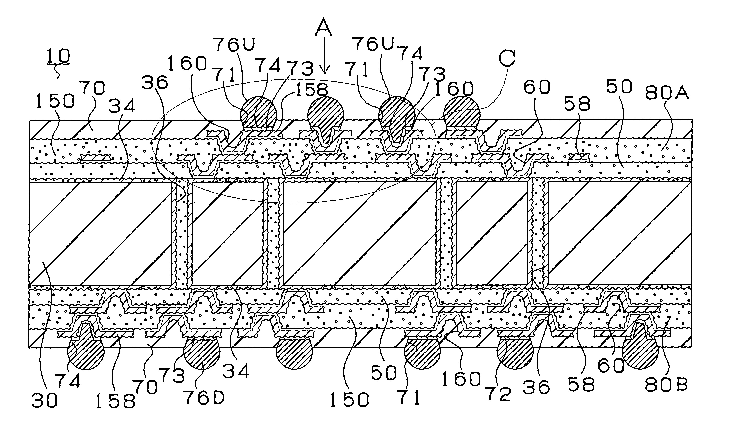
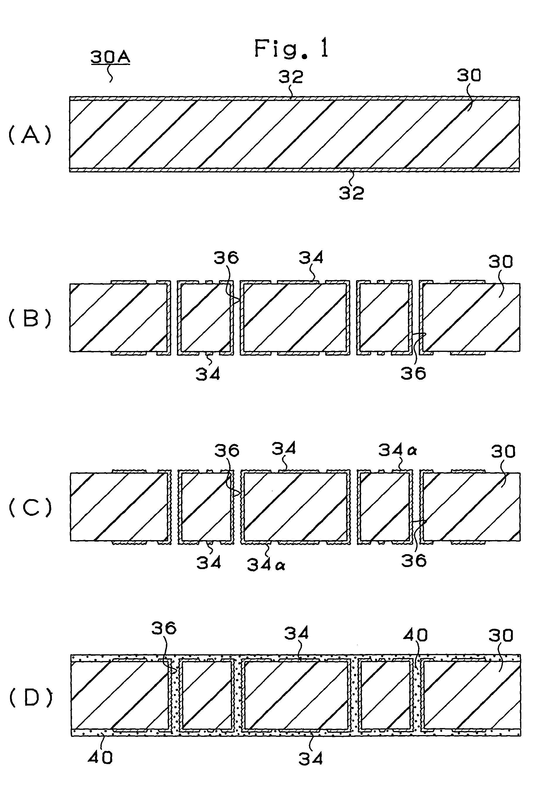
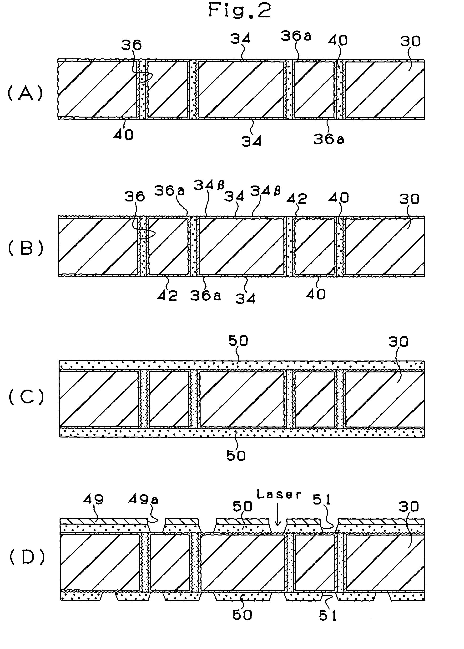
[0099]The configuration of a printed wiring board according to the first embodiment of the present invention will first be described with reference to FIGS. 6 to 9. FIG. 6 shows the cross-section of a printed wiring board 10, and FIG. 7 shows a state in which an IC chip 90 is mounted on the printed wiring board shown in FIG. 6 and attached to a daughter board 94-side.

[0100]As shown in FIG. 6, the printed wiring board 10 has buildup wiring layers BOA and 80B formed on the front and rear surfaces of a core substrate 30, respectively. Each of the buildup wiring layers 80A and 80B comprises of an interlayer resin insulating layer 50 on which conductor circuits 158 and vias 160 are formed, and an interlayer resin insulating layer 150 on which conductor circuits 158 and vias 160 are formed. The buildup wiring layer 80A and the buildup wiring layer 80B are connected through holes 36 formed in the core substrate 30. A solder resist layer 70 is formed on the interlayer resin insulating layer...

second embodiment

[0178]The second embodiment of the present invention will be described hereinafter with reference to the drawings.

[0179]The configuration of a printed wiring board according to the second embodiment of the present invention will first be described with reference to FIGS. 24 to 26. FIG. 24 shows the cross-section of a printed wiring board 10, and FIG. 25 shows a state in which an IC chip 90 is mounted on the printed wiring board shown in FIG. 24.

[0180]As shown in FIG. 24, the printed wiring board 10 has buildup wiring layers 80A and 80B formed on the front and rear surfaces of a core substrate 30, respectively. Each of the buildup wiring layers 80A and 80B comprises of an interlayer resin insulating layer 50 on which conductor circuits 58 and vias 60 are formed, and an interlayer resin insulating layer 150 on which conductor circuits 158 and vias 160 are formed. The buildup wiring layer 80A is connected to the buildup wiring layer 80B via through holes 36 formed in the core substrate...

third modification

[Third Modification]

[0191]A printed wiring board 110 according to the third modification of the present invention will next be described with reference to FIG. 32. In the second embodiment stated above, each solder pad 73 comprises of the tin layer 74 formed on the conductor circuit 158 or via 160. In the third modification, by contrast, the solder pad 73 comprises of a gold layer 174 formed on the conductor circuit 158 or via 160. In the third modification, noble metal is used to coat the conductor circuits 158 and the vias 160, thus ensuring that the solder pads 73 have excellent corrosion resistance. In addition, the use of gold lower in resistance than tin can further increase high frequency characteristic, as compared with the first embodiment.

[0192]The thickness of the gold layer 174 is desirably 0.01 to 3 μm. If the thickness is less than 0.01 μm, portions which cannot completely cover the conductor circuit 158 or via 160 are generated, adversely influencing strength and corr...


PUM

PropertyMeasurementUnit
frequencyaaaaaaaaaa
frequencyaaaaaaaaaa
thicknessaaaaaaaaaa

Abstract

A printed wiring board including solder pads excellent in frequency characteristic is provided. To do so, each solder pad 73 is formed by providing a single tin layer 74 on a conductor circuit 158 or a via 160. Therefore, a signal propagation rate can be increased, as compared with a printed wiring board of the prior art on which two metal layers are formed. In addition, due to lack of nickel layers, manufacturing cost can be decreased and electric characteristics can be enhanced.

Description

TECHNICAL FIELD[0001]This invention relates to a printed wiring board suitable for use as a package substrate, and particularly relates to a printed wiring board having a solder bump formed in each opening of an organic resin insulating layer (a solder resist layer), a printed wiring board having a BGA (ball grid array) connected to each opening through a solder, and a printed wiring board having a conductive connection pin attached, through a conductive adhesive, to a conductor circuit opened and exposed.BACKGROUND ART[0002]A printed wiring board employed as a package substrate is manufactured by a method disclosed in, for example, JP H0 9-130050 A. Electroless plating or etching is conducted on the surface of a conductor circuit for a printed wiring board, thereby forming a roughened layer. Thereafter, the roughened layer is coated with interlayer insulating resin, exposed, and developed by a roll coater and printed to form via hole opening portions for interlayer continuity, and ...

Claims


Application Information

Patent Timeline
Patent Type & Authority Patents(United States)
IPC IPC(8): H01L21/44C23C18/54H01L21/48H01L21/60H01L23/498H01L23/538H05K1/11H05K3/24H05K3/28H05K3/34H05K3/38H05K3/46
CPCC23C18/54H01L23/498H01L23/49816H01L23/49822H01L23/538H01L24/81H05K3/244H05K1/115H01L21/486Y10T29/49147H01L2224/13111H01L2224/16237H01L2224/81801H01L2924/01012H01L2924/01013H01L2924/0102H01L2924/01025H01L2924/01029H01L2924/0103H01L2924/01033H01L2924/01046H01L2924/01051H01L2924/01058H01L2924/01061H01L2924/01078H01L2924/01079H01L2924/01082H01L2924/01322H01L2924/14H01L2924/15311H01L2924/15312H01L2924/19041H05K1/112H05K3/28H05K3/3463H05K3/383H05K3/4602H05K3/4644H01L2924/01005H01L2924/01006H01L2924/01019H01L2924/01023H01L2924/01047H01L2924/0105H01L2924/01067H01L2924/01074H01L2924/014H01L2224/81026H01L2224/81192H01L2924/12042H01L2224/45144H01L2224/05573H01L2224/05568H01L2924/00014H01L2924/00H01L2224/05599
Inventor NAKAI, TORU
Owner IBIDEN CO LTD
Why Eureka
Try Eureka