Eureka AIR delivers breakthrough ideas for toughest innovation challenges, trusted by R&D personnel around the world.

Bit rate-independent optical receiver

Inactive Publication Date: 2006-10-31
SAMSUNG ELECTRONICS CO LTD
View PDF7 Cites 4 Cited by
  • Summary
  • Abstract
  • Description
  • Claims
  • Application Information

AI Technical Summary

Benefits of technology

[0009]The present invention is therefore directed to a bit rate-independent optical receiver capable of ensuring transparency with respect to changes in the transmission format and its associated bit rate in relation to an optical communications system.
[0011]The present invention is still further directed to a bit rate-independent optical receiver that is capable of providing a wider range of bit rates of the optical signals recognizable in an optical communications system.
[0013]Preferably, the amplifier circuit further includes a low-noise amplifier for eliminating noise from the electrical signal outputted from the opto-electric converter and for amplifying the noise-free electrical signal by a given amplification factor; and, a limiting amplifier for re-amplifying the amplified electrical signal within a predetermined voltage level.

Problems solved by technology

However, the aforementioned optical receiver usually does not adapt easily to any changes in the transmission format and its bit rate (so-called “transparency”).
Thus, it has drawbacks in that it is not applicable to optical communications systems in which more than one transmission format is intended for use, and a frequent change in the transmission format is required.
Furthermore, such non-transparency makes it difficult for the optical communications system to perform a real-time monitoring operation in relation to any deteriorative accumulation of the optical signals, such as amplification noise occurring in between network sections, non-linearity of the optical signals, dispersion of color, etc.
Therefore, it causes a considerable limitation in some practical applications of optical networks, i.e., optical line dividers.

Method used


Image

  • Bit rate-independent optical receiver
  • Bit rate-independent optical receiver
  • Bit rate-independent optical receiver

Examples


Embodiment Construction

[0026]In the following description, for purposes of explanation rather than limitation, specific details are set forth such as the particular architecture, interfaces, techniques, etc., in order to provide a thorough understanding of the present invention. However, it will be apparent to those skilled in the art that the present invention may be practiced in other embodiments, which depart from these specific details. For the purpose of simplicity and clarity, detailed descriptions of well-known devices and methods are omitted so as not to obscure the description of the present invention with unnecessary detail.

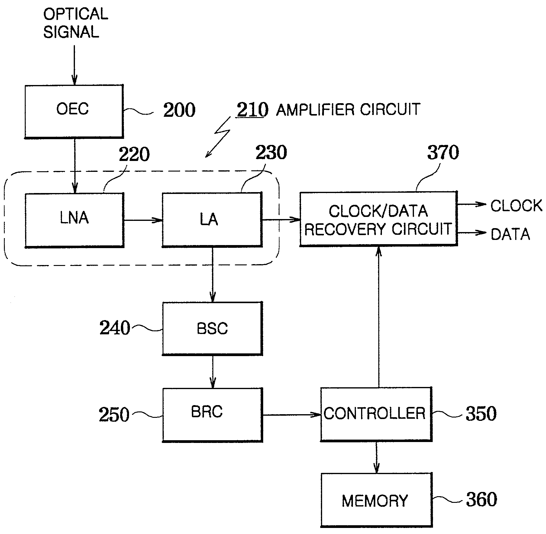
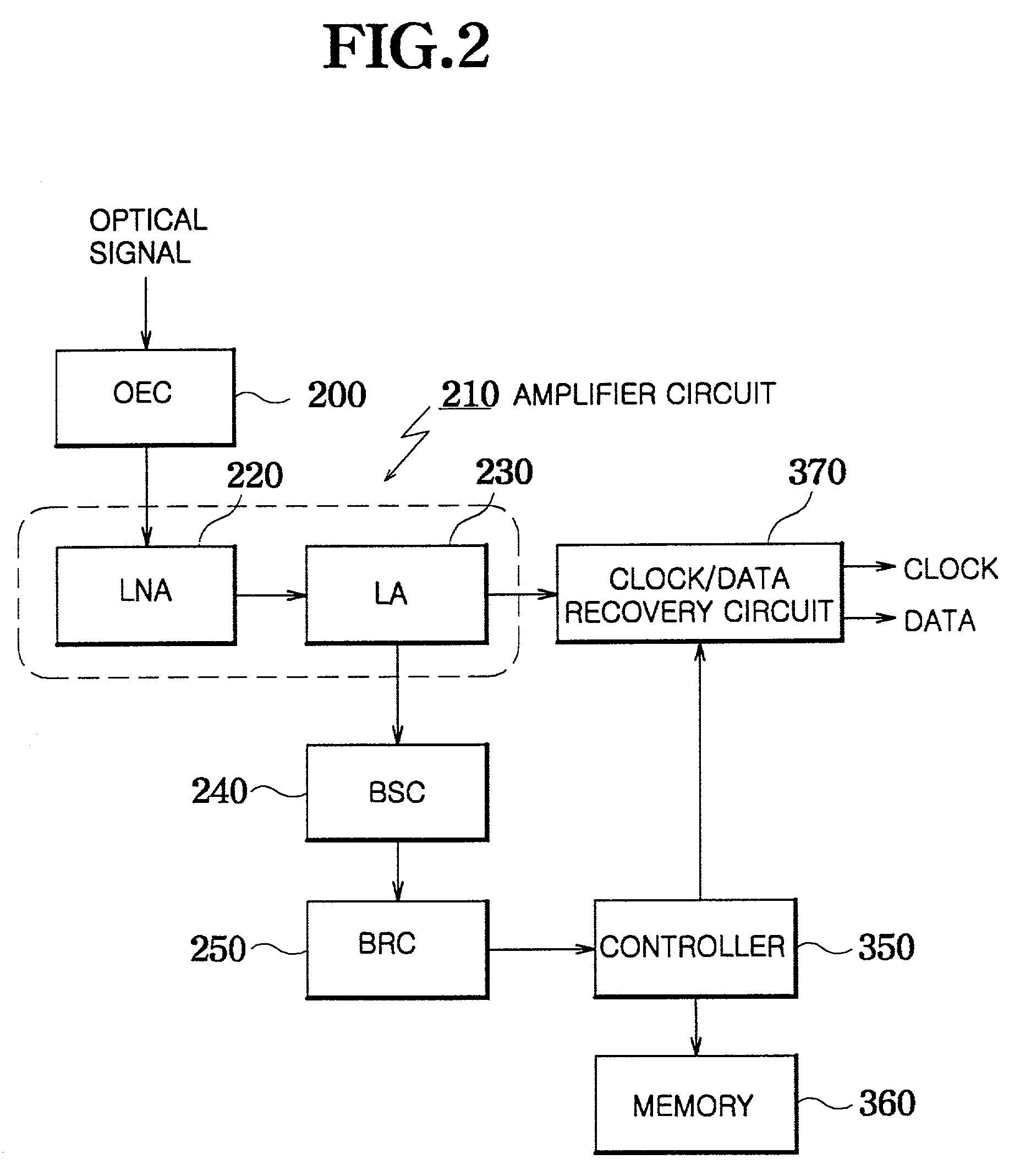
[0027]Referring now to FIG. 2, the optical receiver, according to a preferred embodiment of the present invention, includes an opto-electric converter 200, an amplifier 210, a bit rate-sensing circuit 240, a bit rate-recognition circuit 250, a clock / data recovery circuit 370, a memory 360 and a controller 350.

[0028]In operation, the opto-electric converter 200 converts an inp...


PUM


Abstract

A bit rate-independent optical receiver ensures transparency with respect to changes of the transmission format and its associated bit rate in relation to an optical communications system. The optical receiver includes an opto-electric converter for converting an input optical signal into an electric signal, an amplifier circuit for amplifying the electrical signal, a bit rate-sensing circuit for generating a sensing signal with a voltage level determined on the basis of the bit rate of the electrical signal, a bit rate-recognition circuit for generating a recognition signal further amplified from the sensing signal, and a clock / data recovery circuit for reproducing a clock signal and data from the amplified electrical signal in accordance with a control signal. A controller determines a bit rate corresponding to the voltage level of the recognition signal by referring to a look-up table of the bit rate to the voltage level and provides the clock / data recovery circuit with the control signal representative of the bit rate.

Description

CLAIM OF PRIORITY[0001]This application makes reference to and claims all benefits accruing under 35 U.S.C. Section 119 from an application for “Bit Rate-Independent Optical Receiver,” filed in the Korean Industrial Property Office on Jul. 23, 2001 and there duly assigned Serial No. 44093 / 2001.BACKGROUND OF THE INVENTION[0002]1. Field of the Invention[0003]The present invention relates to optical communications systems and, in particular, to a bit rate-independent optical receiver for use in optical communications systems.[0004]2. Description of the Related Art[0005]In general, optical transmission systems are provided with various communications protocols, i.e., Fiber-Distributed Data Interface (FDDI), Enterprise Systems Connectivity (ESCON), Fiber Channel, Gigabit Ethernet and / or Asynchronous Transfer Mode (ATM). These protocols operate at different bit rates, including 125 Mb / s, 155.520 Mb / s, 200 Mb / s, 622.080 Mb / s, 1062.500 Mb / s, 1.25 Gb / s or 2488.320 Gb / s, etc. As a predetermin...

Claims


Application Information

Patent Timeline
IPC IPC(8): H04B10/00H04B10/40H04B10/07H04B10/2507H04B10/50H04B10/60H04B10/69H04L7/033
CPCH04B10/6932H04B10/60H04B10/69
Inventor CHO, KYU-HYOUNGOH, YUN-JEKOH, JUN-HOKIM, BYUNG-JIKKIM, CHAN-YOULLEE, CHANG-HYUN
Owner SAMSUNG ELECTRONICS CO LTD
Why Eureka
Eureka Blog
Learn More