
Specimen topography reconstruction

Inactive Publication Date: 2006-11-14
ADE CORPORATION
View PDF15 Cites 4 Cited by
  • Summary
  • Abstract
  • Description
  • Claims
  • Application Information

AI Technical Summary

Benefits of technology

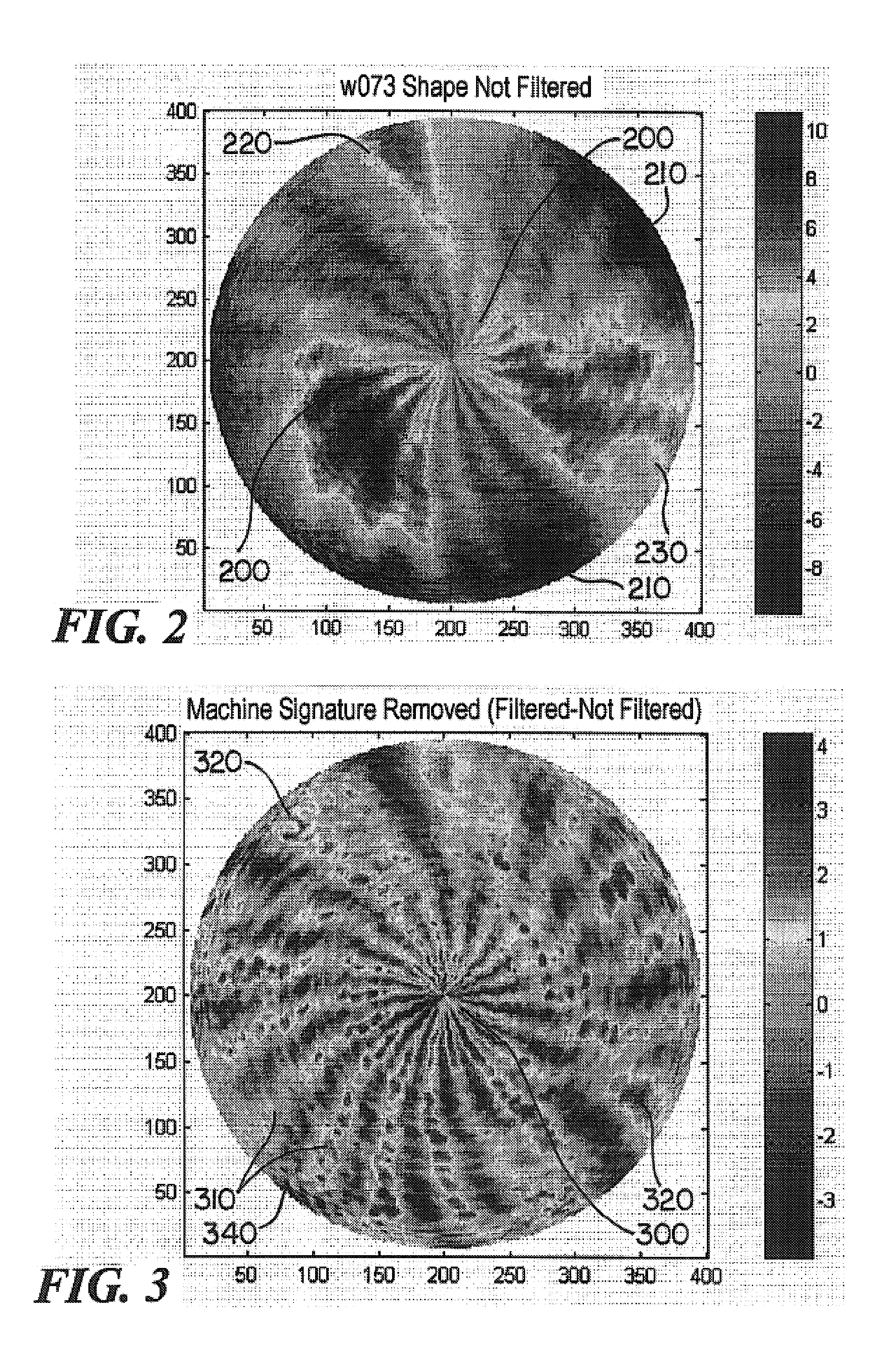
[0009]The invention provides a method to reduce the noise in metrological data from a specimen's topography. The model-based method allows wafer shape reconstruction from data measured by a dimensional metrology system by quantifying the noise in the measurements. The method is based on decomposition of the wafer shape over the full set of spatial measurements. A weighted least squares fit provides the best linear estimate of the decomposition coefficients for a particular piece of test equipment. The fact that wafer's noise is predominantly a low frequency spatial object guarantees fast convergence. An important advantage of the use of the least squares fit method is the fact that a regular grid of data points is not required to calculate the coefficients. Zernike polynomials are preferred for wafer shape reconstruction, as they operate with data that is not taken at regular data points and that represents circular objects.
[0011]Data characterizing the topography of a specimen, in the form of Zernike coefficients, can be sent with specimens or telecommunicated anywhere. Because the Zernike coefficients are a complete characterization and are efficient in using minimum data space, this method significantly improves metrology system performance by removing high frequency noise from the shape data and providing a very compact representation of the shape.

Problems solved by technology

The high accuracy metrology of test specimens, such as the topographic measurement of bow, warp, flatness, thickness etc. of such objects as semiconductor wafers, magnetic disks and the like, is impeded by the presence of noise in the output data.
It is difficult to remove all sources of wafer vibration in a sensor based dimensional metrology system when the wafer moves between the sensors.
If this noise is not removed, it directly affects the repeatability and reproducibility of the measurements of the system.
The positions of those points are not rigorously controlled between specimens.
This limits the usefulness of such noise elimination techniques as correlation analysis.
Similarly the desire to process data for noise reduction from arbitrary shapes, particularly circular, reduces the attractiveness of high speed data systems such as Fast Fourier Transforms.
Because of this requirement for regular data and a priori information, conventional filters such as convolution techniques are not applicable for wafer shape vibration-noise removal.
Fast Fourier transforms are an alternate high speed data processing method, but they are not well adapted to noise reduction processing from arbitrary non-rectilinear shapes, particularly circular shapes.

Method used


Image

  • Specimen topography reconstruction
  • Specimen topography reconstruction
  • Specimen topography reconstruction

Examples


Embodiment Construction

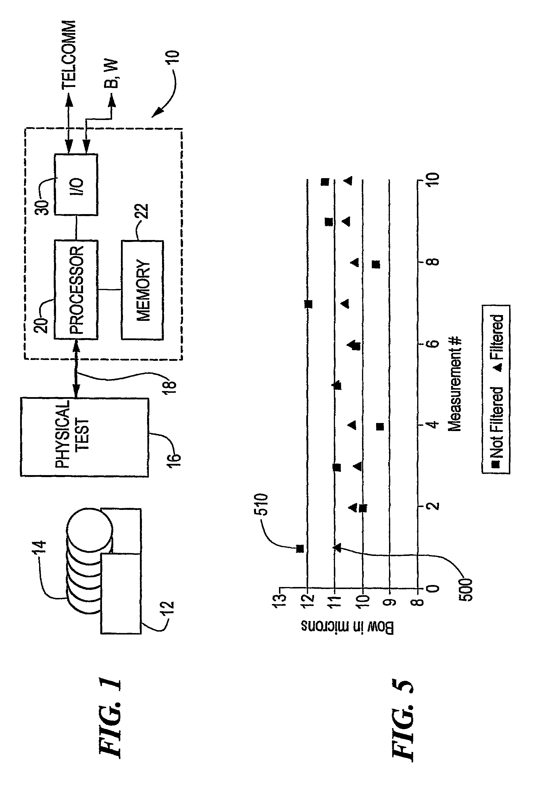
[0018]According to the present invention, and as shown in FIG. 1, a metrology system 10 receives a cassette 12 of semiconductor wafers 14 for testing of surface properties, such as those noted above. The wafers 14 are measured in a physical test apparatus 16, such as any of the ADE Corporation's well-known measurement stations, the WAFERCHECK™ systems being one such.

[0019]The physical test apparatus 16 outputs data to a processor 20 on a communications line 18. The data is typically a vector of measured wafer artifacts, such as flatness height, developed during a spiral scan of the wafer. The present invention operates to eliminate or reduce the noise from the wafer measurement system.

[0020]The raw noisy data is typically stored in a memory area 22 where its vector can be represented as W(ρ, φ), where ρ is the normalized (r / radius) radial location of each measurement point, and θ is the angle in polar coordinates of the measurement point. The processor 20 performs a transform on thi...


PUM


Abstract

This method removes high frequency noise from shape data, significantly improves metrology system (10) performance and provides very compact representation of the shape. This model-based method for wafer shape reconstruction from data measured by a dimensional metrology system (10) is best accomplished using the set of Zernike polynomials (matrix L). The method is based on decomposition of the wafer shape over the complete set of the spatial function. A weighted least squares fit is used to provide the best linear estimates of the decomposition coefficients (Bnk). The method is operable with data that is not taken at regular data points and generates a reduced data field of Zernike coefficients compared to the large size of the original data field.

Description

CROSS REFERENCE TO RELATED APPLICATIONS[0001]This application claims priority of U.S. Provisional Patent Application No. 60 / 174,082 Entitled: SPECIMEN TOPOGRAPHY RECONSTRUCTION filed Dec. 30, 1999, incorporated herein by reference.STATEMENT REGARDING FEDERALLY SPONSORED RESEARCH OR DEVELOPMENT[0002]N / ABACKGROUND OF THE INVENTION[0003]Wafer shape is a geometric characteristic of a semiconductor wafer, which describes the position of the wafer's central plane surface in space. The bow, warp and other shape related parameters of semiconductor wafers must be within precise tolerances in order for wafers to be usable. The precision of a dimensional metrology (measurement) system must be tight enough to provide the required control over the quality of manufactured wafers.[0004]The high accuracy metrology of test specimens, such as the topographic measurement of bow, warp, flatness, thickness etc. of such objects as semiconductor wafers, magnetic disks and the like, is impeded by the prese...

Claims


Application Information

Patent Timeline
IPC IPC(8): G06K9/00G01B11/24G06T7/60H01L21/66
CPCG06T7/606H01L22/20G06T2207/30148G06T7/66
Inventor SINHA, JAYDEEPBELYAEV, ALEXANDER
Owner ADE CORPORATION
Learn More