Semiconductor wafer, polishing apparatus and method

Inactive Publication Date: 2006-11-21
GLOBALWAFERS CO LTD
View PDF16 Cites 23 Cited by
  • Summary
  • Abstract
  • Description
  • Claims
  • Application Information

AI Technical Summary

Benefits of technology

[0008]Among the several objects and features of the present invention may be noted the provision of a semiconductor wafer, semiconductor wafer polishing apparatus and method which improves the flatness of the wafers processed; the provision of such a wafer, apparatus and method which reduces wafer ed

Problems solved by technology

Presently, flatness parameters of the polish surfaces of single side polished wafers are typically acceptable within a central portion of most wafers, but the flatness parameters become unacceptable near the edges of the wafers, as described below.
The construction of conventional polishing machines contributes to unacceptable flatness measurements near the wafer's edge.
A change in the net vertical force applied to the wafer locally changes the polishing pressure and the polishing rate of the wafer, giving rise to distortions in the polish.
Often the uneven forces cause the wafer's peripheral edge margin to be slightly thinner than the majority of the wafer, rendering the

Method used


Image

  • Semiconductor wafer, polishing apparatus and method
  • Semiconductor wafer, polishing apparatus and method
  • Semiconductor wafer, polishing apparatus and method

Examples


first embodiment

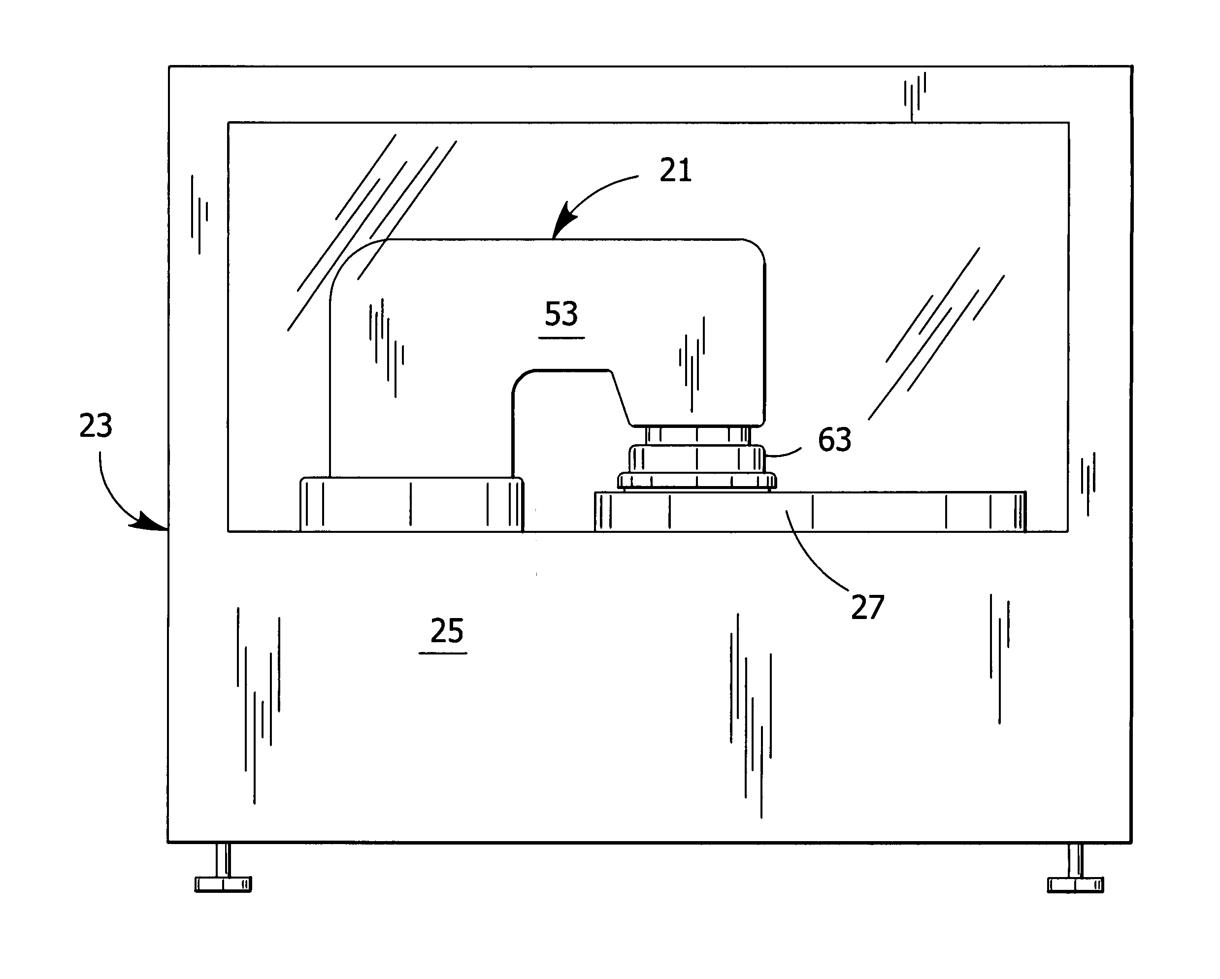
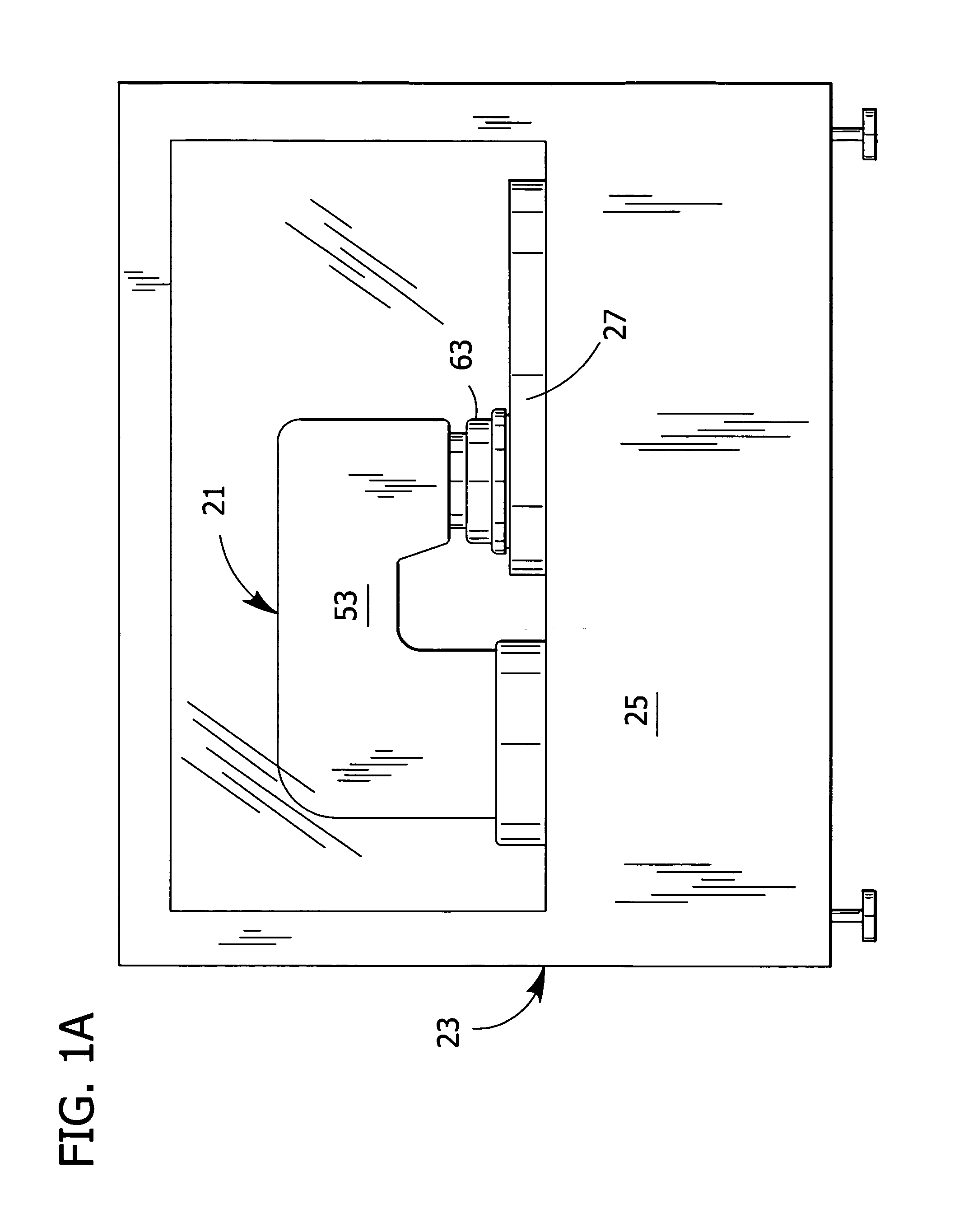
[0040]The wafer polishing apparatus 21 further comprises a semi-rigid connection, generally indicated at 89, between the drive mechanism 45 and the polishing head 63 for imparting a rotational force from the drive mechanism to the polishing head (FIG. 1B). The semi-rigid connection 89 ensures that the polishing head 63 and drive mechanism 45 rotate conjointly so the control device can regulate the speed of the drive mechanism, and thereby the rotation of the wafer 35. Without the semi-rigid connection 89, the upper bearing member 77 would rotate with the drive mechanism 45 while the lower bearing member 79 and wafer 35 would fail to rotate beneath the spherical bearing assembly 75. The connection between the drive mechanism 45 and the polishing head 63 must be semi-rigid so that the universal pivoting motion of the polishing head with respect to the drive mechanism about the spherical bearing assembly 75 is unaffected by the driving force of the drive mechanism. The semi-rigid conne...

second embodiment

[0047]Turning to the polishing head of the present invention, a polishing head 153 connects to the drive mechanism 45 for driven rotation of the polishing head (FIG. 3). The polishing head 153 is adapted to hold a wafer 35 for engaging a front surface 39 of the wafer with a work surface 37 of the polishing pad 29. The polishing head 153 is attached to the drive mechanism 45 via a spherical bearing assembly, generally indicated at 159, for pivoting of the polishing head about a gimbal point lying near the work surface 37. The polishing head 153 holds the front surface 39 of the wafer 35 in engagement with the polishing pad 29, thereby polishing the wafer and allowing the plane of the front surface to continuously align itself to equalize polishing pressure over the front surface of the wafer for more uniform polishing of a semiconductor wafer.

[0048]A semi-rigid connection, generally indicated at 163, attaches to the drive mechanism 45 and the polishing head 153 for transferring a rot...

third embodiment

[0054]Turning to the polishing head, the present embodiment comprises a polishing head 223 connected to the drive mechanism 45 for driven rotation of the polishing head (FIG. 4). The polishing head 223 is adapted to hold a wafer 35 for engaging a front surface 39 of the wafer 35 with a work surface 37 of the polishing pad. Like the previous embodiment, the present embodiment is directed to providing uniform pressure over the wafer 35 for removal of a uniform layer of silicon from a wafer made flat by a double-side polishing process or a fine grinding process.

[0055]A spherical bearing assembly, generally indicated at 227, connects the polishing head 223 and the drive mechanism 45 for pivoting of the polishing head. The spherical bearing assembly further comprises an upper conical seat 229 and a lower spherical pivot 231, similar to the second embodiment. The upper conical seat 229 is preferably welded to the drive mechanism 45 along a distal end 232 of the drive mechanism, although o...


PUM

PropertyMeasurementUnit
Fractionaaaaaaaaaa
Fractionaaaaaaaaaa
Fractionaaaaaaaaaa

Abstract

A wafer polishing apparatus for polishing a semiconductor wafer. The polisher comprises a base (23), a turntable (27), a polishing pad (29) and a drive mechanism (45) for driven rotation of a polishing head (63). The polishing head is adapted to hold at least one wafer (35) for engaging a front surface of the wafer with a work surface of the polishing pad. A spherical bearing assembly (75) mounts the polishing head (63) on the drive mechanism for pivoting of the polishing head about a gimbal point (p) lying no higher than the work surface when the polishing head holds the wafer in engagement with the polishing pad. This pivoting allowing the plane of the front surface of the wafer to continuously align itself to equalize polishing pressure over the front surface of the wafer, while rotation of the polishing head is driven by the driving mechanism. This maintains the front surface and work surface in a continuously parallel relationship for more uniform polishing of a semiconductor wafer, particularly near the lateral edge of the wafer. A cassette of wafers and method of polishing are also disclosed.

Description

BACKGROUND OF THE INVENTION[0001]This invention relates to apparatus for polishing semiconductor or similar type materials, and more specifically to such apparatus which facilitates equalization of the downward pressure over the polished wafer surface and / or the polishing head of the apparatus.[0002]Polishing an article to produce a surface which is highly reflective and damage free has application in many fields. A particularly good finish is required when polishing an article such as a wafer of semiconductor material in preparation for printing circuits on the wafer by an electron beam-lithographic or photolithographic process (hereinafter “lithography”). Flatness of the wafer surface on which circuits are to be printed is critical in order to maintain resolution of the lines, which can be as thin as 0.13 microns (5.1 microinches) or less. The need for a flat wafer surface, and in particular local flatness in discrete areas on the surface, is heightened when stepper lithographic p...

Claims


Application Information

Patent Timeline
IPC IPC(8): B24B1/00B24B37/30B24B41/04B24B49/00H01L21/304H01L21/673
CPCB24B37/30B24B41/04B24B49/006H01L21/304
Inventor BOVIO, EZIOCORBELLINI, PARIDEMORGANTI, MARCONEGRI, GIOVANNIALBRECHT, PETER D.
Owner GLOBALWAFERS CO LTD
Why Eureka
Try Eureka