
Semiconductor device and method of manufacturing the same

Inactive Publication Date: 2006-11-21
RENESAS ELECTRONICS CORP
View PDF9 Cites 19 Cited by
  • Summary
  • Abstract
  • Description
  • Claims
  • Application Information

AI Technical Summary

Benefits of technology

[0008]An Object of the present invention is to provide a flip-chip semiconductor device whose manufacturing cost is reduced by reusing a supporting substrate having high rigidity when a multilayer wiring board is formed, and the method of manufacturing a semiconductor device.
[0010]In the present invention, after the etching-back layer and the multilayer wiring board were formed on the supporting substrate, the etching-back layer is etched to remove the supporting substrate from the multilayer wiring board. Accordingly, the semiconductor chip is mounted on the multilayer wiring board to manufacture a semiconductor device, and also the supporting substrate is removed so that it can be reused. As a result, the manufacturing cost of the semiconductor device can be reduced.
[0012]A semiconductor device according to the present invention has a multilayer wiring board and a semiconductor chip mounted on the multilayer wiring board. The semiconductor chip is mounted on the multilayer wiring board. The multilayer wiring board is separated from a supporting substrate by etching an etching-back layer. The etching-back layer is formed between the multilayer wiring board and the supporting substrate. Accordingly, the present invention can provide inexpensive semiconductor devices.
[0013]As described above, according to the present invention, after the multilayer wiring board was formed on a supporting substrate through an etching-back layer, the etching-back layer was etched so that the supporting substrate can be removed from the multilayer wiring board. As a result the supporting substrate can be reused and a material cost in the manufacturing cost of a semiconductor device can be significantly decreased. Thus, the cost of the semiconductor manufactured by the use of the multilayer wiring board can be reduced.

Problems solved by technology

However, the above-described conventional arts have the following problems.
Accordingly, when the next multilayer wiring board is formed, a new supporting substrate must be prepared, which results in increased cost.

Method used


Image

  • Semiconductor device and method of manufacturing the same
  • Semiconductor device and method of manufacturing the same
  • Semiconductor device and method of manufacturing the same

Examples


first embodiment

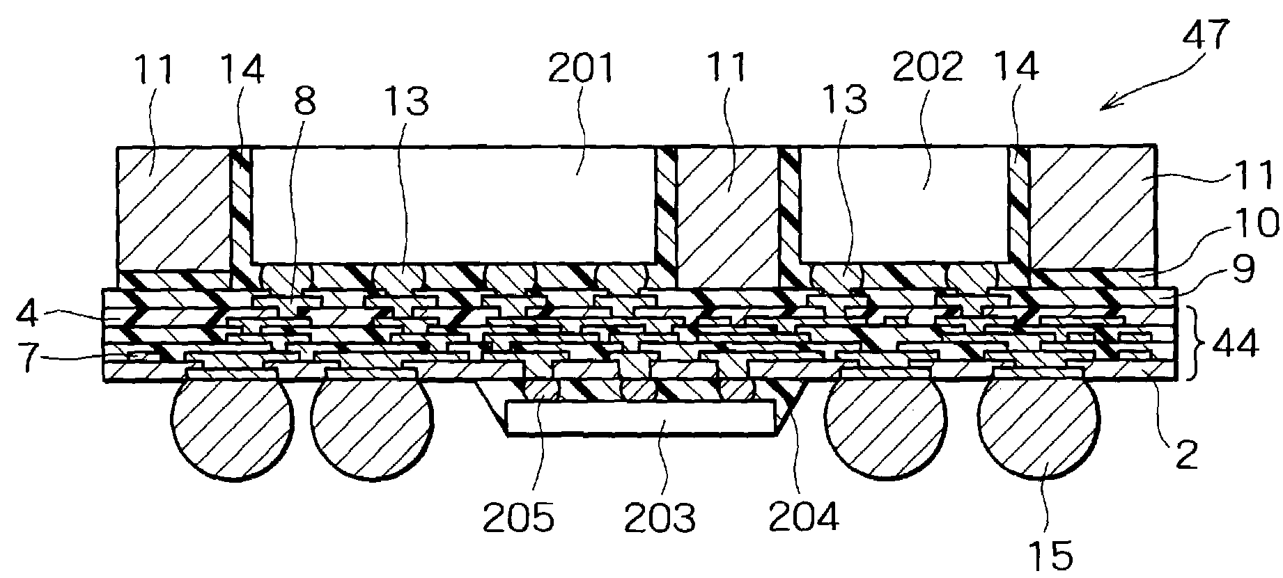
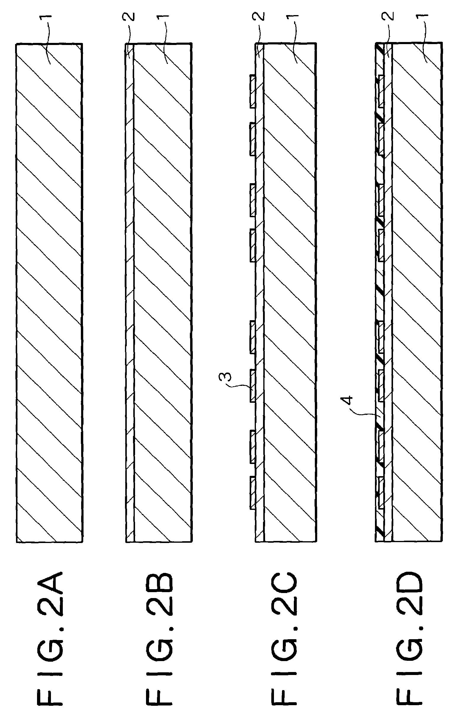
[0025]Embodiments of the present invention will now be described in detail with reference to attached drawings. First, the present invention will be described. FIGS. 2A to 2G, FIGS. 3A to 3F, FIGS. 4A to 4D, and FIGS. 5A to 5D are cross-sectional views showing a method of manufacturing a semiconductor device according to the present embodiment.

[0026]First, as shown in FIG. 2A, a base substrate 1 having high surface flatness and high mechanical strength is prepared. A material forming this base substrate 1 is a material having an elastic modulus of, for example, 20 GPa or more, and more preferably 100 GPa or more at room temperature. The materials of the base substrate 1 are for example, metals or alloy materials such as Si, Ti alloys, stainless steels (SUS), duralumin, maraging steel and the like, or inorganic ceramic materials such as alumina. mullite, aluminum nitride, and the like, or organic materials having excellent surface flatness and heat-resisting properties such as polyim...

second embodiment

[0080]Further, if etching-back layers are formed on both front and back surfaces of the base substrate like the above-mentioned second embodiment and multilayer wiring boards are formed on the etching-back layers, the throughput per one base substrate becomes twice and a remarkable improvement of the manufacturing efficiency becomes possible. As a result, a drastic reduction in the manufacturing cost for the semiconductor devices becomes possible.


PUM


Abstract

The present invention relates to a method of manufacturing a semiconductor device. In the method, an etching-back layer consisting of aluminum or copper is formed on a base substrate and a multilayer wiring board is manufactured on the etching-back layer. After that the etching-back layer is etched to be removed under the condition that the multilayer wiring board and the base substrate are not etched, so that the base substrate is separated from the multilayer wiring board. Accordingly, the base substrate can be reused.

Description

BACKGROUND OF THE INVENTION[0001]1. Field of the Invention[0002]The present invention relates to a semiconductor device whose manufacturing cost was reduced and method of manufacturing the same, and particularly relates to a flip-chip type semiconductor device in which a semiconductor chip was mounted on a multilayer wiring board and method of manufacturing the same.[0003]2. Description of the Related Art[0004]As disclosed in Japanese Patent Publication Laid-open No. 2001-257288, in accordance with the demands of weight reduction in a semiconductor device and a reduction of a mounting area, semiconductor devices, particularly flip-chip type semiconductor devices, which are assembled by a bare chip mounting process have been noted.[0005]FIG. 1 is a cross-sectional view showing a conventional flip-chip type semiconductor device. As shown in FIG. 1, in the conventional flip-chip type semiconductor device 318, an insulating substrate 311 is provided. And a conductive adhesive 313 is pro...

Claims


Application Information

Patent Timeline
IPC IPC(8): H01B13/00H01L21/48H01L23/12H01L21/68H01L23/31H01L23/36H05K3/20H05K3/46
CPCH01L21/4857H01L21/6835H05K3/20H01L24/97H01L2924/07802H01L2924/19106H01L2224/73253H01L2224/73204H01L2224/32225H01L2224/16225H01L2924/01024H01L2924/01006H05K3/4644H01L2924/18161H01L2924/15311H01L2924/1517H01L2924/15153H01L23/3128H01L2221/68345H01L2224/16H01L2224/97H01L2924/01004H01L2924/01005H01L2924/01011H01L2924/01013H01L2924/01029H01L2924/0103H01L2924/01033H01L2924/01042H01L2924/01046H01L2924/01047H01L2924/01074H01L2924/01077H01L2924/01078H01L2924/01079H01L2924/01082H01L2924/1433H01L2224/81H01L2924/00H01L21/52
Inventor HONDA, HIROKAZU
Owner RENESAS ELECTRONICS CORP
Learn More