Electron-emitting device, electron source, and image display apparatus
Inactive Publication Date: 2006-11-21
CANON KK
View PDF20 Cites 3 Cited by
Summary
Abstract
Description
Claims
Application Information
AI Technical Summary
This helps you quickly interpret patents by identifying the three key elements:
Problems solved by technology
Method used
Benefits of technology
Benefits of technology
[0020]In the case of (2), a structure of the carbon fiber and a formation density thereof can be made relatively uniform. However, as shown in FIG. 10, the edge portions 95 are formed at the edge regions of the patterned area. In the edge portions 95, the electric field enhancing effect resulting from electric field concentration generally becomes larger, so that a threshold voltage to the electron emission reduces.
[0023]The present invention has been made to solve the above-mentioned problems. An object of the present invention is to provide an electron-emitting device, and an electron source, which can be used to manufacture an image forming apparatus having a superior display quality and in which the development of the abnormal light emission point is suppressed and the non-uniformity of brightness is not caused.
[0058]According to the present invention, it is possible to provide an electron-emitting device in which an electron-emitting characteristic distribution in the electron-emitting region is small and to reduce a variation in electron-emitting characteristic between electron-emitting devices. Therefore, by using electron source in which a plurality of electron-emitting devices according to the present invention are arranged, an image forming apparatus capable of uniformly displaying an image having a preferable quality on a large area is obtained.
Problems solved by technology
However, with respect to the device formed by the micro fabrication, it is difficult to increase the number of devices per pixel in the image display apparatus.
However, there is a limitation on sharpening of the tip portion by a micro fabrication technique and it is difficult to reduce an electric field strength required for field emission.
Method used
Image
Click on the blue label to locate the original text in one second.
Reading with bidirectional positioning of images and text.
Examples
example 1
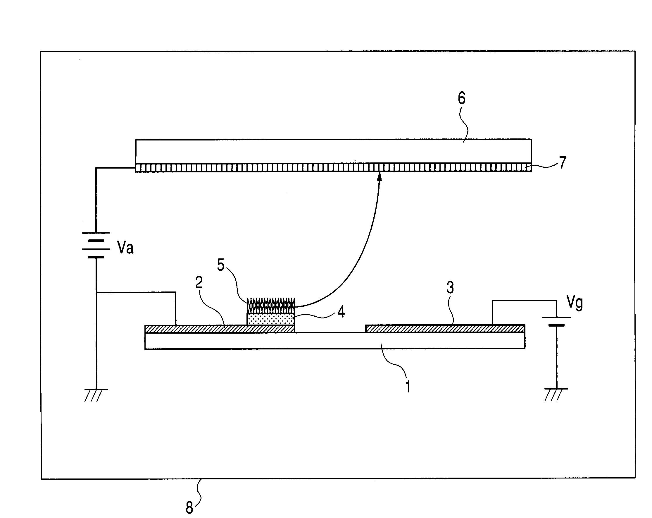
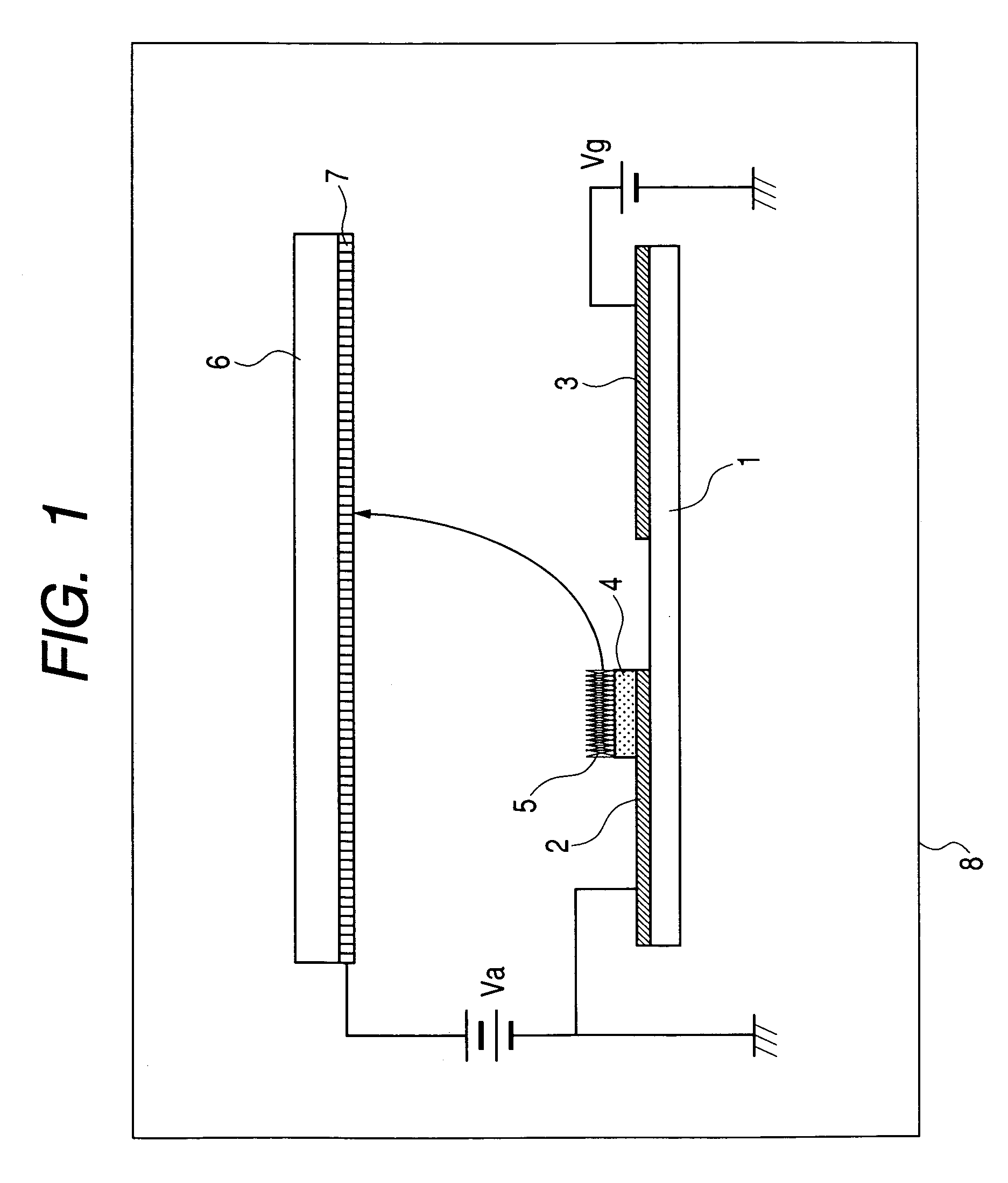
[0107]FIG. 2 shows the electron-emitting device according to Example 1 when it is viewed from above the base surface.
[0108]In FIG. 2, reference numeral 1 denotes the substrate; 2, the cathode electrode; 3, the gate electrode; and 5, the electron-emitting film. Note that the conductive layer 4 (not shown) is inserted between the cathode electrode 2 and the electron-emitting film 5, and a combination of the cathode electrode 2 and the conductive layer 4 is called the cathode electrode.
[0109]Here, quartz is used for the substrate 1, Pt is used for the cathode electrode 2 and the gate electrode 3, a graphitenanofiber is used for the electron-emitting film 5, and TiN is used for the conductive layer 4.
[0110]Also, according to the structure shown in FIG. 2, the conductive layer 4 and the electron-emitting film 5 are formed in substantially the same region. However, the conductive layer 4 may be formed so as to include a formation region of the electron-emitting film 5.
[0111]The electron-...
example 2
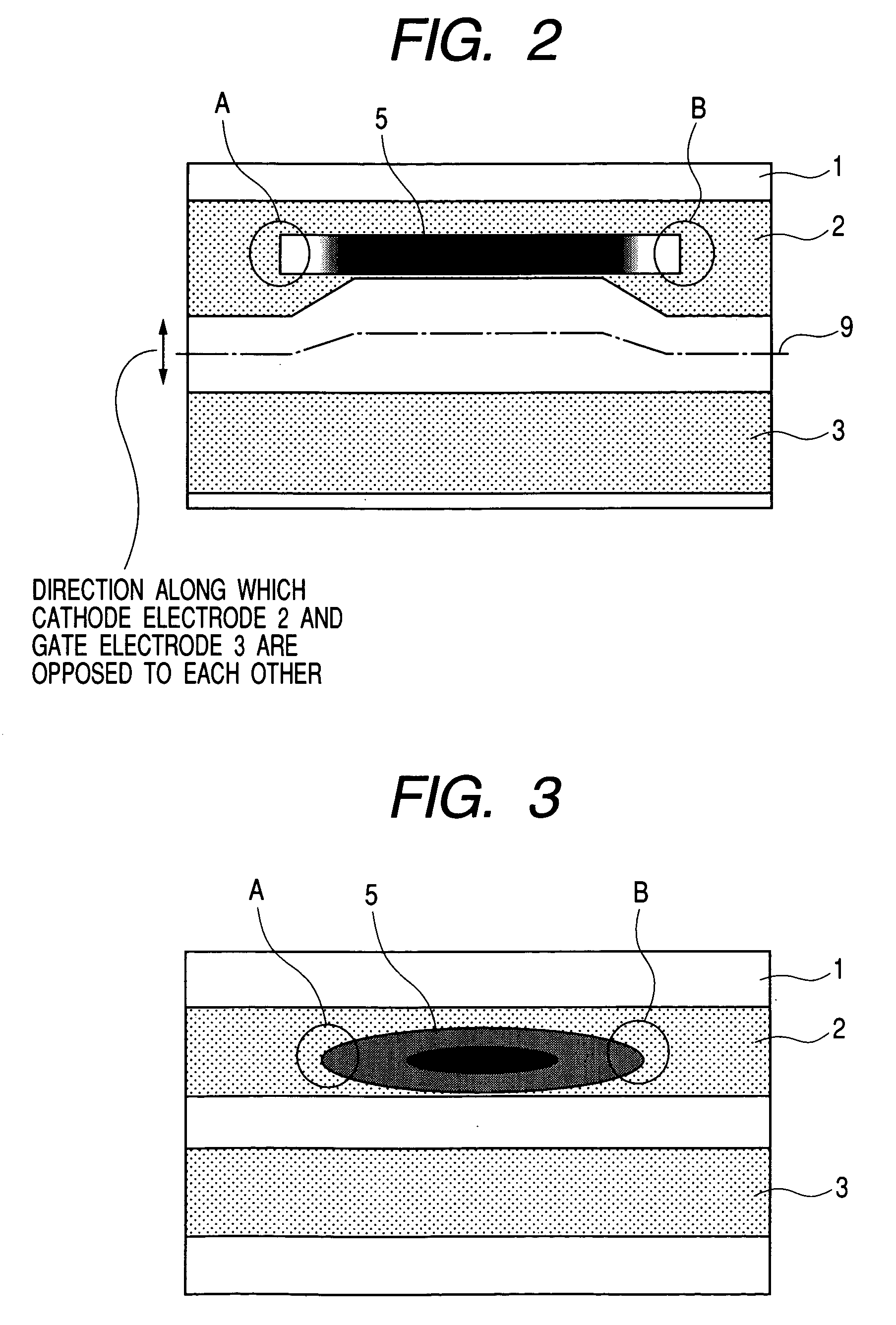
[0124]FIG. 3 shows the electron-emitting device according to Example 2 when it is viewed from above the base surface. The electron-emitting device according to this example can be manufactured by the same method as for the electron-emitting device described in Example 1. In addition, the same references are provided to the same members as in Example 1.
[0125]In the electron-emitting device according to this example, the space between the gate electrode 3 and the cathode electrode 2 is constant. The electron-emitting film 5 was elliptically patterned and the substantially two end portions A and B exist in a direction along a gap between the gate electrode 3 and the cathode electrode 2.
[0126]As is apparent from FIG. 3, the distance between the end of the cathode electrode 2 and the electron-emitting film 5 is relatively large in each of the end portions A and B. On the other hand, in the region between the end portions A and B, the end of the cathode electrode 2 is close to the end of ...
example 3
[0130]FIG. 4 shows the electron-emitting device according to Example 3 when it is viewed from above the base surface. The electron-emitting device according to this example can be manufactured by the same method as for the electron-emitting device described in Example 1. In addition, the same references are provided to the same members as in Example 1.
[0131]The electron-emitting film 5 was patterned in a strip shape with a predetermined width. Therefore, the two end portions A and B exist in the longitudinal direction of the electron-emitting film 5.
[0132]The cathode electrode 2 protrudes more to the gate electrode 3 side in areas between each of the two end portions A and B of the electron-emitting film 5 and the gate electrode 3, as compared with an area between the region located between the two end portions of the electron-emitting film 5 and the gate electrode 3.
[0133]Thus, the space between the gate electrode 3 and the cathode electrode 2 is not constant but is wider in the re...
PUM
Abstract
To provide an electron-emitting device that can be used to manufacture an image forming apparatus having a superior display quality and in which the development of the abnormal light emission point is suppressed and the unevenness of brightness is not caused. The electron-emitting device includes: a cathodeelectrode and a gate electrode, which are formed on a base surface and opposed to each other with a space therebetween; and an electron-emitting film which is located on the cathodeelectrode, and in the electron-emitting device, the electron-emitting film has two end portions (A and B) in a plane substantially parallel to the base surface in a direction substantially perpendicular to a direction along which the cathode electrode and the gate electrode are opposed to each other, and a structure is used in which electric field strengths applied between each of the two end portions (A and B) of the electron-emitting film and the gate electrode are made weaker than an electric field strength applied between a region between the two end portions (A and B) of the electron-emitting film and the gate electrode at a time of driving.
Description
BACKGROUND OF THE INVENTION[0001]1. Field of the Invention[0002]The present invention relates to an electron-emitting device having a film containing an electron-emitting material, an electron source in which a large number of electron-emitting devices are arranged, and an image display apparatus using the electron source.[0003]2. Related Background Art[0004]Recently, a carbon fiber such as a carbon nanotube (hereinafter referred to as a “CNT”) serving as a cold cathode material is attracting attention. The carbon nanotube is a fullerene having a cylindrical structure in which graphite of several layers or a single layer is wound, and is a new carbon material discovered in 1991 (Nature, 354, (1991) 56). Further, an application of a carbon nanotube to an image display apparatus using an electron source in which a large number of minute electron-emitting devices are two-dimensionally formed is being attempted.[0005]Up to now, there has been known an example of a field emission type el...
Claims
Application Information
Patent Timeline
Application Date:The date an application was filed.
Publication Date:The date a patent or application was officially published.
First Publication Date:The earliest publication date of a patent with the same application number.
Issue Date:Publication date of the patent grant document.
PCT Entry Date:The Entry date of PCT National Phase.
Estimated Expiry Date:The statutory expiry date of a patent right according to the Patent Law, and it is the longest term of protection that the patent right can achieve without the termination of the patent right due to other reasons(Term extension factor has been taken into account ).
Invalid Date:Actual expiry date is based on effective date or publication date of legal transaction data of invalid patent.

