ALD of tantalum using a hydride reducing agent

a technology of hydride reducing agent and tantalum, which is applied in the direction of coating, chemical vapor deposition coating, metallic material coating process, etc., can solve the problems of reducing resistance, poor adhesion of copper seed layer (and copper in general) to the underlying diffusion barrier layer, and diffusion barrier materials that are not sufficiently conductive to support direct electroplating of copper. , to achieve the effect of reducing hydrid

Inactive Publication Date: 2006-12-05
NOVELLUS SYSTEMS
View PDF13 Cites 160 Cited by
  • Summary
  • Abstract
  • Description
  • Claims
  • Application Information

AI Technical Summary

Benefits of technology

[0008]The present invention provides an ALD process using a tantalum-halide precursor and a hydride reducing agent to deposit a thin, highly conformal tantalum or tantalum-containing film. The methods include using a tantalum halide to deposit a saturated layer of tantalum precursor onto a substrate, then contacting the tantalum precursor with a hydride reducing agent (a silicon hydride or a boron hydride, for example) to form a thin layer of tantalum-containing material (tantalum metal or tantalum silicide or tantalum boride, for example). This composes one cycle of the ALD process. Another thin conformal layer of tantalum-containing material can then be deposited on top of this newly formed tantalum layer by introducing more of the tantalum halide and then introducing more reducing hydride. It may be desirable to purge the reaction chamber with inert gas between each reactant exposure and after each successive deposition cycle. Subsequent layers can be added to create a tantalum-containing material layer with a desired thickness to within about 3 angstroms.

Problems solved by technology

Copper atoms are rather mobile and can easily diffuse or migrate into the supporting dielectric and thereby reduce its resistance.
The diffusion barrier materials are not sufficiently conductive to support direct electroplating of copper from solution.
One problem encountered in the above process involves poor adhesion of the copper seed layer (and copper in general) to the underlying diffusion barrier layer.
It turns out that copper does not adhere well to the diffusion barrier materials.
In fact, copper does not adhere well to a wide array of materials employed in integrated circuits.
Unfortunately, there are currently no thermal CVD processes available for depositing tantalum films at temperatures below 450 degrees C.
Thus, many useful CVD precursors are not viable as ALD precursors, and it is not trivial to select a precursor for the ALD method.
In a metal ALD process, it is especially challenging to find a metal precursor that is stable against decomposition, adsorbs evenly on the surface and can also be easily reduced.

Method used


Image

  • ALD of tantalum using a hydride reducing agent
  • ALD of tantalum using a hydride reducing agent
  • ALD of tantalum using a hydride reducing agent

Examples


Embodiment Construction

[0019]Introduction

[0020]In the following detailed description of the present invention, numerous specific embodiments are set forth in order to provide a thorough understanding of the invention. However, as will be apparent to those skilled in the art, the present invention may be practiced without these specific details or by using alternate elements or processes. In other instances well-known processes, procedures and components have not been described in detail so as not to unnecessarily obscure aspects of the present invention.

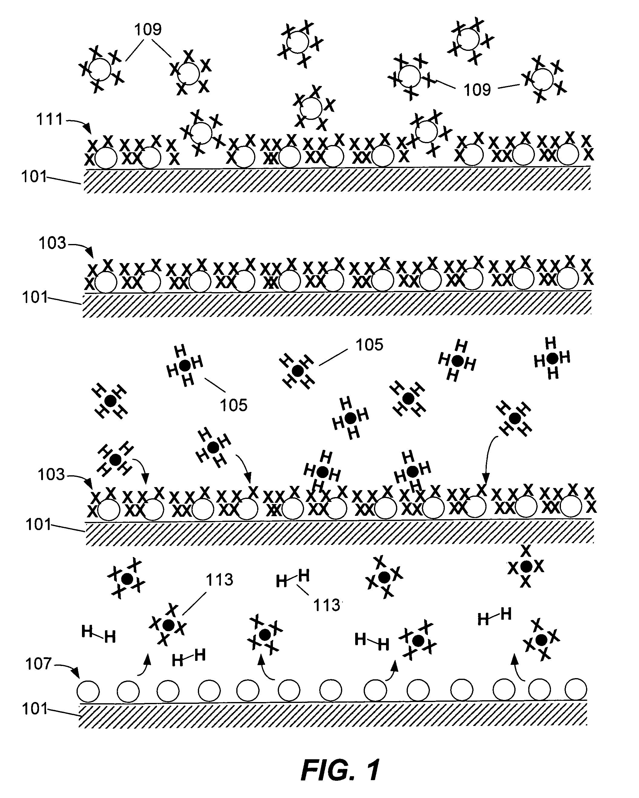
[0021]Atomic layer deposition (ALD) can be considered a variant of the well-established chemical vapor deposition (CVD), but based on separated surface-controlled reactions. In ALD, reactants are directed alternately over a substrate surface as depicted in FIG. 1, separated by purging steps using an inert gas or other method. ALD relies on the chemisorption of a gaseous precursor 109 (a tantalum halide in this case) to form a “saturated layer” of the precu...


PUM

PropertyMeasurementUnit
temperaturesaaaaaaaaaa
thicknessaaaaaaaaaa
thicknessaaaaaaaaaa

Abstract

An ALD method deposits conformal tantalum-containing material layers on small features of a substrate surface. The method includes the following principal operations: depositing a thin conformal and saturated layer of tantalum-containing precursor over some or all of the substrate surface; using an inert gas or hydrogen plasma to purge the halogen byproducts and unused reactants; reducing the precursor to convert it to a conformal layer of tantalum or tantalum-containing material; using another purge of inert gas or hydrogen plasma to remove the halogen byproducts and unused reactants; and repeating the deposition/reduction cycles until a desired tantalum-containing material layer is achieved. An optional step of treating each newly formed surface of tantalum containing material with a nitrogen-containing agent can be added to create varying amounts of tantalum nitride.

Description

FIELD OF THE INVENTION[0001]This invention pertains to methods for tantalum and tantalum containing material deposition. More specifically, the invention pertains to methods that deposit a layer of tantalum or tantalum silicide material on a semiconductor device to improve adhesion between deposited copper metal and an underlying diffusion barrier, for example.BACKGROUND OF THE INVENTION[0002]Damascene processes for forming integrated circuit metalization layers employ electroplated copper lines formed in vias and trenches of supporting dielectric layers. Copper atoms are rather mobile and can easily diffuse or migrate into the supporting dielectric and thereby reduce its resistance. To address this problem, damascene processes employ thin diffusion barrier layers on the entire exposed surface of the dielectric. These barrier layers are made from a material that effectively blocks transport of copper atoms into the adjacent dielectric. Typically, the barrier layers comprise slightly...

Claims


Application Information

Patent Timeline
Patent Type & Authority Patents(United States)
IPC IPC(8): H01L21/44H01L21/4763H01L21/8242
CPCC23C16/14C23C16/38C23C16/42C23C16/45542H01L21/28562H01L21/76843
Inventor FAIR, JAMES A.SUNG, JUNGWANTAYLOR, NERISSA
Owner NOVELLUS SYSTEMS
Why Eureka
Try Eureka