Laminating double-side circuit board, manufacturing method thereof, and multilayer printed circuit board using same

a technology of printed circuit board and double-side, which is applied in the field of laminated double-side circuit board, manufacturing method thereof, and multi-layer printed circuit board using same. it can solve the problems of complex manufacturing process, limitation of high-density packaging of electronic components, and insufficiently meeting the requirements of wiring board, so as to reduce the manufacturing process and simplify the manufacturing process. , the effect of reliable laminated board structur

Inactive Publication Date: 2006-12-19
PANASONIC CORP
View PDF12 Cites 26 Cited by
  • Summary
  • Abstract
  • Description
  • Claims
  • Application Information

AI Technical Summary

Benefits of technology

[0026]Thus, the present invention can provide a multilayer printed wiring board that has a reli...

Problems solved by technology

This imposes limitation to high-density packaging of electronic components.
Thus, this poses problem that such a wiring board cannot sufficiently meet the requirements of microminiaturization of portable electronic equipment, and commercial use of a narrow pitch package and a multi chip module (MCM), for example.
(1) For multi-layering, the process of lamination by hot-pressing and the process of patterning copper foils by etching ...

Method used


Image

  • Laminating double-side circuit board, manufacturing method thereof, and multilayer printed circuit board using same
  • Laminating double-side circuit board, manufacturing method thereof, and multilayer printed circuit board using same
  • Laminating double-side circuit board, manufacturing method thereof, and multilayer printed circuit board using same

Examples


Embodiment Construction

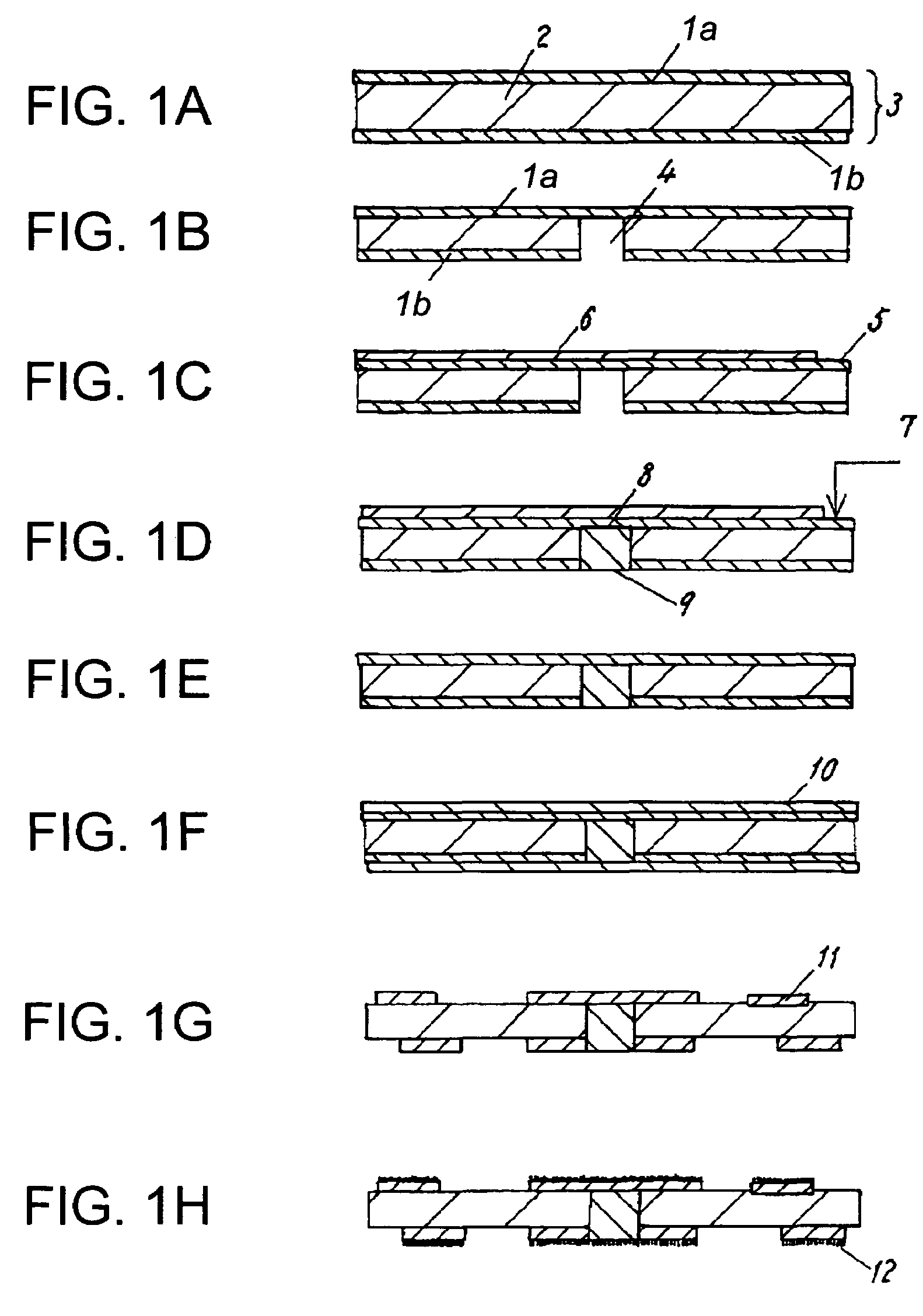
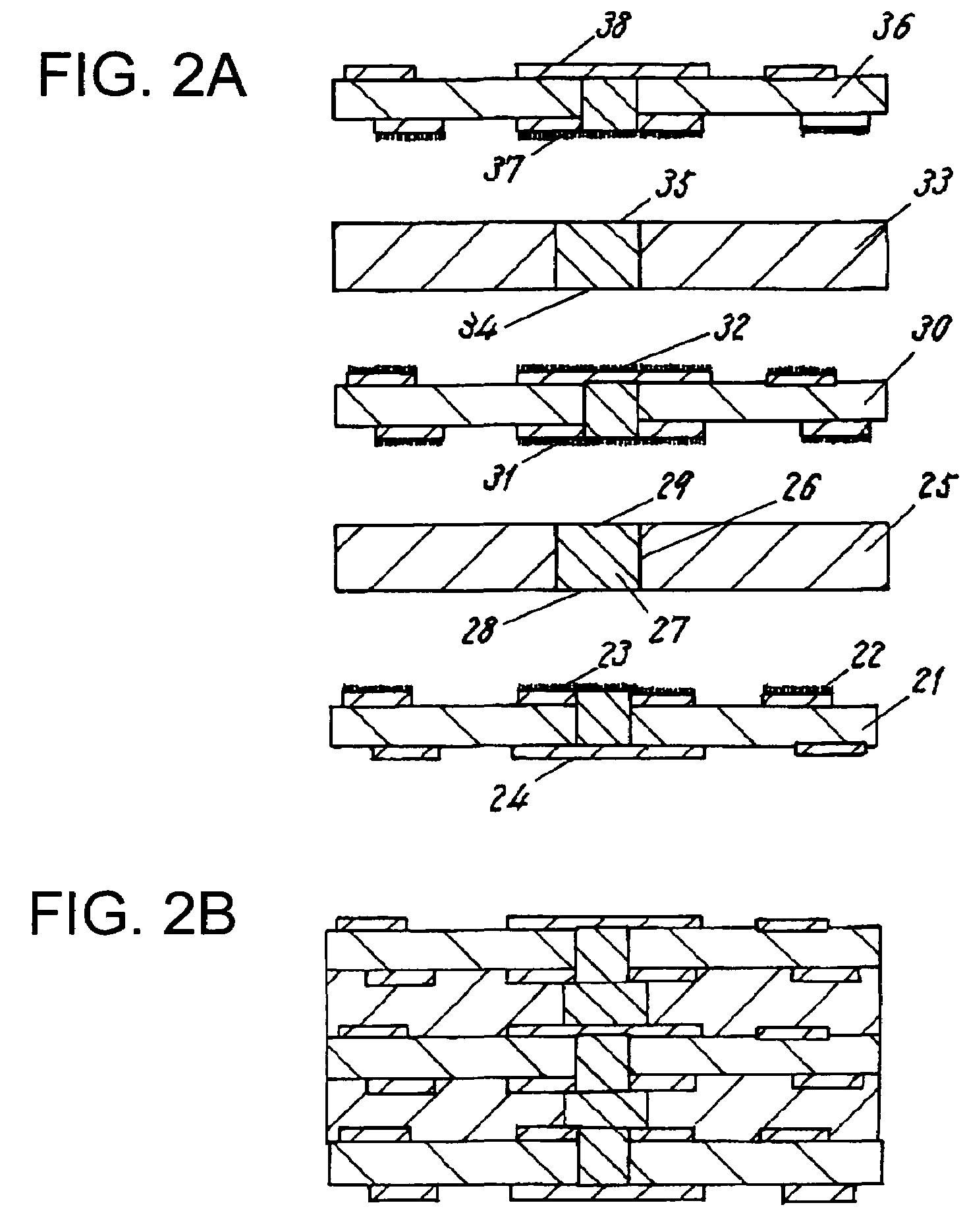
[0030]Exemplary embodiments of a laminating double-side circuit board and a multilayer printed wiring board of the present invention are demonstrated hereinafter with reference to FIGS. 1A to 1H.

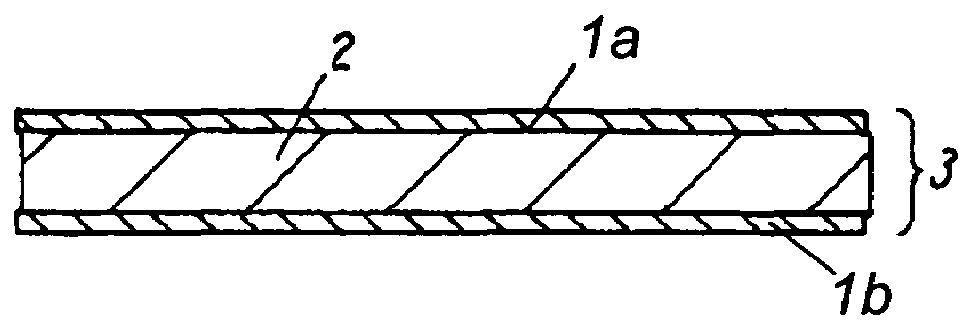
[0031]First, as shown in FIG. 1A, metal layers 1a and 1b are adhered to each side of insulated substrate 2 to form double-side copper-clad laminate 3. The insulated substrate is made of an insulating material selected from epoxy resin impregnated glass-cloth substrate, epoxy resin impregnated aramid-unwoven cloth substrate, polyimide resin impregnated glass-cloth substrate, polyimide resin impregnated aramid-unwoven cloth substrate, bismaleimide-triazine resin laminate, and the like.

[0032]Copper foils can be used as metal layers 1a and 1b adhered to both sides of insulated substrate 2. Preferably, copper foils are treated to have roughened surfaces to improve adhesive properties thereof.

[0033]Alternatively, metal layers 1a and 1b can be copper deposit formed on the surfaces of insulated subs...


PUM

PropertyMeasurementUnit
Diameteraaaaaaaaaa
Lengthaaaaaaaaaa
Lengthaaaaaaaaaa

Abstract

The present invention comprises a plurality of laminating double-side circuit boards and a plurality sheets of prepreg for interlayer connection that are placed one on another. Via holes extend from the circuit on one side of each laminating double-side circuit board to the circuit on the other side thereof. Each via hole is filled with electro-conductive material to connect the circuits on both sides of the laminating double-side circuit board. The pad on a laminating double-side circuit board and the pad on another laminating double-side circuit board are laminated via a sheet of prepreg for interlayer connection so that the respective pads are opposed to each other via the through hole filled with electro-conductive material formed through the sheet of prepreg for interlayer connection. Thereby, the respective pads on the laminating double-side wiring circuit boards are electrically connected with one another. Thus, the present invention can provide a multilayer printed wiring board having shorter production time, excellent reliability, and high yield.

Description

FIELD OF THE INVENTION[0001]The present invention relates to a laminating double-side circuit board used to manufacture a multilayer printed wiring board having an interstitial via hole (IVH) structure. It also relates to a manufacturing method of the circuit board and a multilayer printed wiring board using the circuit boards.BACKGROUND OF THE INVENTION[0002]Commonly, a conventional multilayer printed wiring board is made by alternately placing copper-clad laminates and sheets of prepreg one on another and integrating them. Such a multilayer printed wiring board has circuit patterns having outer layer pads formed therein, on the surfaces of the wiring board, and circuit patterns having inner layer pads formed therein, on the interlayer insulating layers of the wiring board.[0003]These circuit patterns having these pads formed therein are electrically connected with each other via through holes drilled between each wiring layer in the direction of the thickness of the laminate.[0004...

Claims


Application Information

Patent Timeline
IPC IPC(8): H05K1/03H05K3/00H05K3/38H05K3/40H05K3/42H05K3/46
CPCH05K3/462H05K3/0038H05K3/0035Y10T29/49155H05K3/384H05K3/385H05K3/4069H05K3/423H05K3/4623H05K2201/0394H05K2201/10378H05K2203/0554H05K2203/0733H05K2203/108H05K2203/1461
Inventor TAKASE, YOSHIHISANAKAMURA, TSUNESHI
Owner PANASONIC CORP
Why Eureka
Try Eureka