Method and apparatus for calibration of near-field scanning optical microscope tips for laser machining

a scanning optical microscope and probe tip technology, applied in the direction of optical means, instruments, manufacturing tools, etc., can solve the problems of affecting the accuracy of laser machining, and the inability to accurately calibrate the probe tip of the near-field scanning optical microscop

Inactive Publication Date: 2006-12-19
PANASONIC CORP
View PDF2 Cites 7 Cited by
  • Summary
  • Abstract
  • Description
  • Claims
  • Application Information

AI Technical Summary

Problems solved by technology

The feature sizes used to form photonic crystals and the precise alignment requirements of these features complicate manufacture of these materials.
One challenge in producing micro-circuitry is preventing shorts between components and nano-wires which are located ever closer together.
It is noted that other modes than the near-field mode may be transmitted through the NSOM probe tip, but, as long as the probe tip is maintained suitably close to the surface being machined, the possible presence of these other modes does not have a large effect on these advantages of NSOM laser machining.
The wavelength of the laser is still an issue, however, because it affects the efficiency with which the light may be coupled into the near-field through the NSOM probe tip.
An important issue in such a system is ensuring that the laser light is efficiently coupled into, and out of, the NSOM probe.
The probe tip may be imaged in a scanning electron microscope (SEM) and the tip quality assessed based on its appearance, but this method does not provide a direct measurement of the light coupled through the tip.
Thus, it may be difficult, or even impossible, to calibrate the probe tips using SEM images only.
SEM imaging may be desirable to initially screen NSOM probes for defective NSOM tips, but it is impractical for monitoring of the probe tips during operation for wear and / or damage.

Method used


Image

  • Method and apparatus for calibration of near-field scanning optical microscope tips for laser machining
  • Method and apparatus for calibration of near-field scanning optical microscope tips for laser machining
  • Method and apparatus for calibration of near-field scanning optical microscope tips for laser machining

Examples


Embodiment Construction

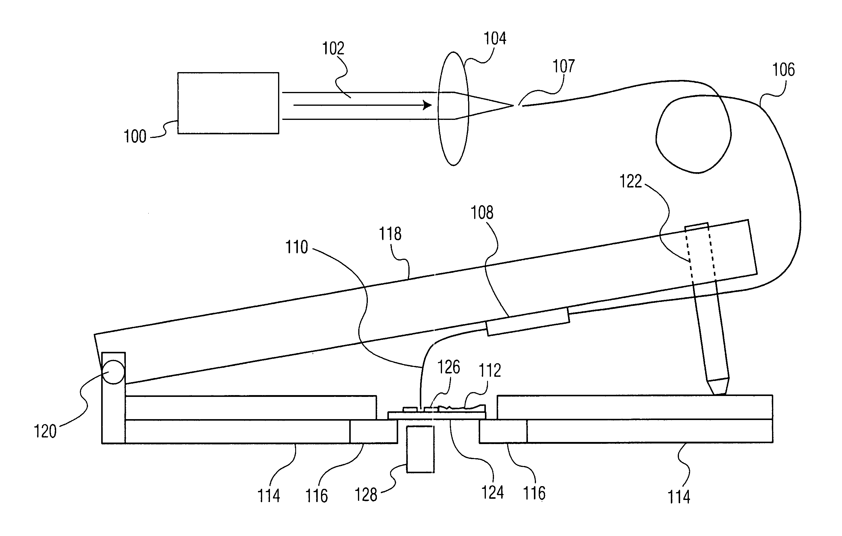
[0029]FIG. 1 illustrates a simplified block diagram of an exemplary NSOM laser machining system of the present invention, including an exemplary means of measuring light coupled through the NSOM probe tip. This light may desirably include near-field mode light evanescently coupled from the NSOM probe tip to a coupling substrate, and may also include far-field mode light or other light coupled through the NSOM probe tip.

[0030]Quantum cellular automata, coupled quantum dot devices, resonant tunneling devices, multifunction optical arrays, diffractive optical elements, beam shapers, microlens arrays, optical diffusers, beam splitters, laser diode correctors, fine pitch gratings, photonic crystals, micro-electrical-mechanical systems, micro-circuitry, micro-surface-acoustic-wave devices, micro-mechanical oscillators, polymerase chain reaction microsystems, biochips for detection of hazardous chemical and biological agents, high-throughput drug screening and selection Microsystems, and m...


PUM

PropertyMeasurementUnit
laser peak wavelengthaaaaaaaaaa
surface areaaaaaaaaaaa
distanceaaaaaaaaaa

Abstract

A system for measuring radiation at a peak wavelength that is radiated from a probe tip of a near-field scanning optical microscope (NSOM) probe used for laser machining, including: a laser source; the NSOM probe; a coupling substrate that is substantially transmissive to the peak wavelength; an NSOM mount to controllably hold the probe and the coupling substrate; an NSOM probe monitor coupled to the mount; an NSOM controller; and a photodetector optically coupled to the substrate. Light is coupled into the probe. The mount includes a Z motion stage. The probe monitor determines the distance between the probe tip and the coupling substrate. The controller is coupled to the probe monitor and the motion stage. It controls the distance between the probe tip and the coupling substrate such that radiation is coupled from the probe tip into the coupling substrate. The photodetector measures the power of this radiation.

Description

FIELD OF THE INVENTION[0001]The present invention concerns an apparatus and method for calibrating the probe tips of a near-field scanning optical microscope (NSOM). This method may also provide for the improved manufacture, mass customization, or repair of electronic, optical, and mechanical microstructures.BACKGROUND OF THE INVENTION[0002]As products get smaller and smaller, there is increased demand for micro-electrical-mechanical systems (MEMS), micro-optical devices and photonic crystals. With this demand, there is an associated increased interest in micro- and nano-machining. Numerous applications exist for MEMS. As a breakthrough technology, allowing unparalleled synergy between previously unrelated fields such as biology and microelectronics, new MEMS applications are emerging at a rapid pace, expanding beyond those currently identified or known. Additional applications in quantum electric devices, micro-optical devices and photonic crystals are also emerging.[0003]Here are ...

Claims


Application Information

Patent Timeline
Patent Type & Authority Patents(United States)
IPC IPC(8): G02B7/04G01Q10/00G01Q40/00G01Q60/18
CPCB23K26/04B23K26/0635B82Y20/00B82Y35/00G01Q40/00G01Q60/22B82Y5/00B23K26/0624
Inventor CHENG, CHEN-HSIUNGLI, MING
Owner PANASONIC CORP
Why Eureka
Try Eureka