Parameter correction circuit and parameter correction method

a correction circuit and parameter technology, applied in the direction of instruments, digital computer details, electric/magnetic computing, etc., can solve the problems of difficult to include the required number of resistors, include resistors, etc., and achieve the effect of high precision and high precision

Inactive Publication Date: 2006-12-19
PANASONIC CORP
View PDF7 Cites 41 Cited by
  • Summary
  • Abstract
  • Description
  • Claims
  • Application Information

AI Technical Summary

Benefits of technology

[0040]As described above, in the present invention, a current is allowed to flow from the mirror circuit connected to the current supply to a reference parameter having a preliminarily known parameter value so that a voltage of the reference parameter at this time is detected, and based upon this voltage, the current value of the current supply is calculated; therefore, even when the current value deviates due to production deviations of the current supply, it is possible to correct the parameter value of the variable parameter in response to a current value of each of the current supplies.
[0041]In particular, in the present invention, even when, upon measuring a voltage of the reference parameter and the variable parameter, the parameter values of the first and second switching circuits give influences on the corresponding voltage value, a current is allowed to flow from the mirror circuit to the third switching circuit in a separated manner so that a voltage of the third switching circuit at this time is measured; therefore, each of the voltages generated in the reference parameter and the variable parameter is reduced by a voltage generated in the above-mentioned third switching circuit so that the influences from the first and second switching circuits can be removed; thus, it becomes possible to carry out the correction on the variable pa...

Problems solved by technology

However, in the case where the resistor 52r is included as such an externally added part, a plurality of resistors 52r need to be included depending on writing speed modes, and since the number of terminals to be prepared in a semiconductor integrated circuit is limited, it is difficult to include resistors 52r, the number of which is the same as the number of the speed modes to be set, as externally added parts.
Moreover, since various recording-type optical disks, such as DVD-Rs ...

Method used


Image

  • Parameter correction circuit and parameter correction method
  • Parameter correction circuit and parameter correction method
  • Parameter correction circuit and parameter correction method

Examples


embodiment 1

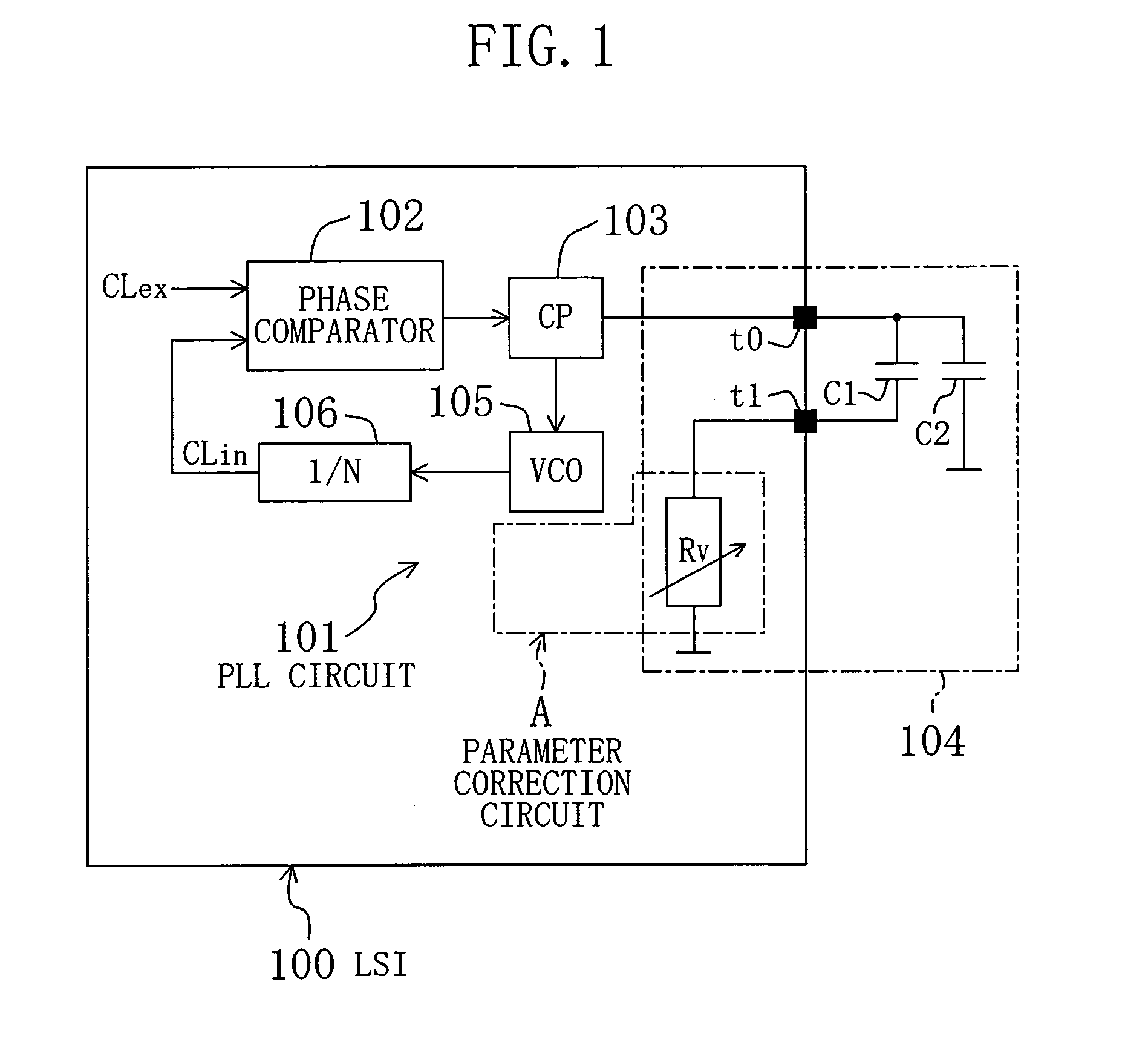
[0057]FIG. 1 shows a schematic structure of a semiconductor integrated circuit that includes a parameter correction circuit in accordance with a first embodiment of the present invention.

[0058]In FIG. 1, reference numeral 100 represents a semiconductor integrated circuit (LSI) used for a data writing / reading system and the like for use in, for example, a recording-type optical disk, and 101 represents a PLL circuit. This PLL circuit 101 is provided with a phase comparator 102, a charge pump circuit 103, a filter circuit 104, a voltage control oscillator 105 and a frequency divider 106. The filter circuit 104 is provided with a variable resistor element Rv and two capacitor elements C1 and C2. The PLL circuit 101 is included inside the above-mentioned semiconductor integrated circuit 100, except the two capacitor elements C1 and C2 of the filter circuit 104. In the filter circuit 104, the two capacitor elements C1 and C2, placed outside the semiconductor integrated circuit 100, are c...

embodiment 2

[0074]Referring to the figures, the following description will discuss a second embodiment of the present invention.

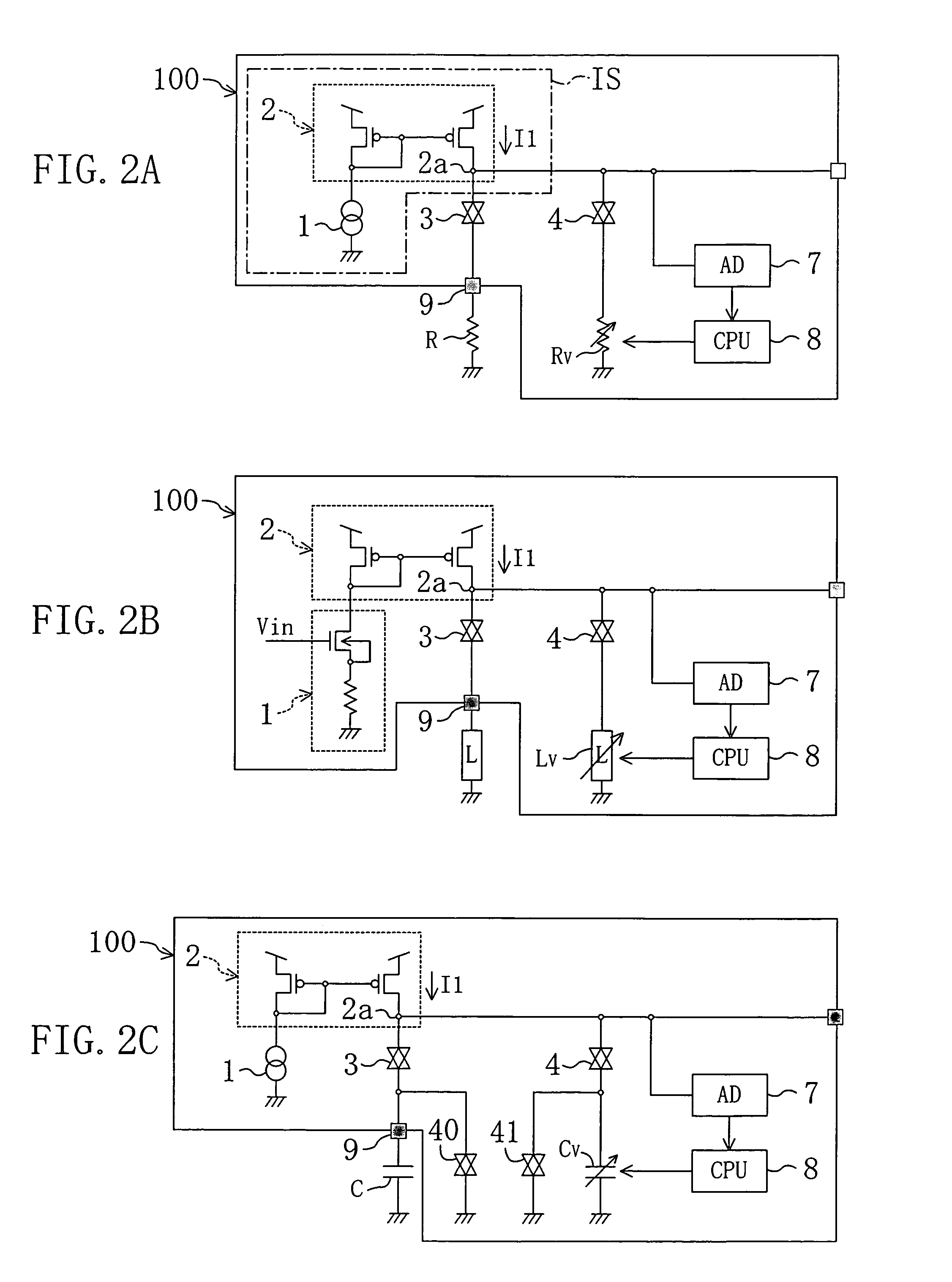
[0075]FIG. 2B shows a structure of a parameter correction circuit in accordance with the second embodiment of the present invention. In this embodiment, an inductor element is used as the parameter.

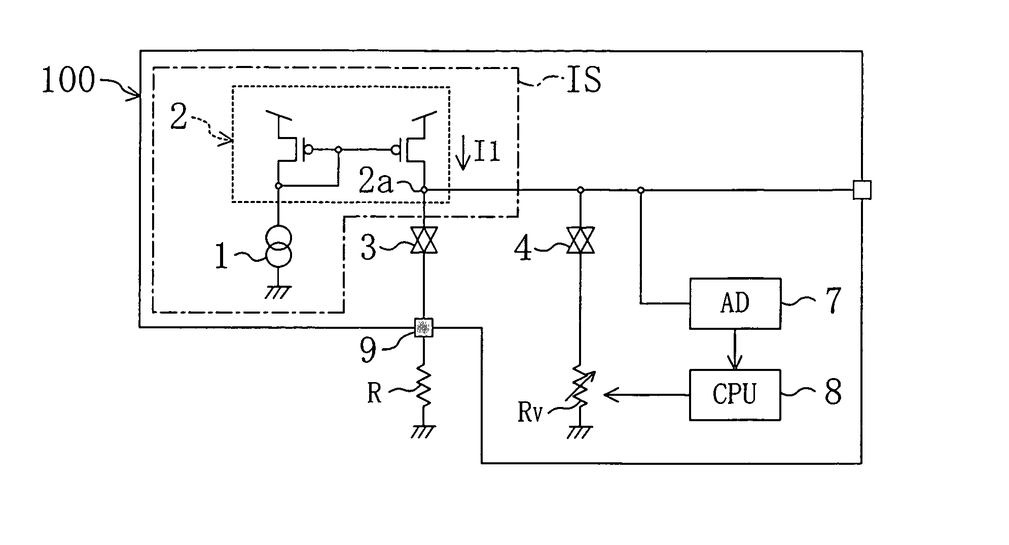
[0076]In FIG. 2B, reference numeral 1 represents a variable current supply that is formed by a source follower constituted a resistor and a transistor, 2 represents a mirror circuit constituted by two p-type transistors that allow a current I1 that is equal to a current from the variable current supply 1 to flow, 3 and 4 represent respectively independent switching circuits, L represents a reference inductor element that is included outside the LSI 100, Lv represents a variable inductor element in which the inductance value can be switched in a range of 0 H to Lv H, 7 represents a voltage measuring circuit and 8 is a CPU.

[0077]In the parameter correction circuit in the prese...

embodiment 3

[0086]Referring to the figures, the following description will discuss a third embodiment of the present invention.

[0087]FIG. 2C shows a structure of a parameter correction circuit in accordance with the third embodiment of the present invention. In this embodiment, a capacitor element is used as the parameter.

[0088]In FIG. 2C, reference numeral 1 represents a current supply, 2 represents a mirror circuit that is constituted by two p-type transistors that allow a current I1 that is equal to a current from the current supply 1 to flow, 3 and 4 represent respectively independent switching circuits, C represents a reference capacitor that is included outside the LSI 100, and Cv represents a variable capacitor in which the capacitance value can be switched in a range from initial 0 F to the maximum Cv F. Here, the maximum value of the capacitance value Cv is indicated by the same sign Cv. Reference numeral 7 represents a voltage measuring circuit, 8 is a CPU, and 40 and 41 are respectiv...


PUM


Abstract

In a parameter correction circuit in an LSI, a reference resistor element with high precision having a resistance value set to a target value is connected to an external terminal of the LSI. A constant current from a mirror circuit connected to a current supply flows through the reference resistor element. A voltage value generated in the reference resistor element is measured by a voltage measuring circuit. The constant current also flows through a variable resistor element. The resistance value of the variable resistor element is adjusted so that a voltage generated in the variable resistor element corresponds to the voltage generated by the reference resistor element.

Description

BACKGROUND OF THE INVENTION[0001]The present invention relates to a parameter correction circuit and a parameter correction method which correct production deviations in parameters of a device such as a resistor element, and are desirably applied to a PLL (Phase Locked Loop) circuit to be included in a semiconductor integrated circuit for use in, for example, a data writing / reading system of a recording-type optical disk.[0002]Conventionally, in a recording-type optical disk, for example, a DVD-R and a DVD-RAM, address signals, referred to as wobble signals, are physically located in its tracks. A PLL circuit, which is included in a semiconductor integrated circuit for use in a data writing / reading system of such a recording-type optical disk, multiplies the wobble signal 186 times to generate a recording clock so that based upon this recording clock, data is written on an recording-type optical disk in an unrecorded state.[0003]Here, as shown in FIG. 10, such a PLL circuit is provi...

Claims


Application Information

Patent Timeline
IPC IPC(8): H03L7/06H03L7/093H03L7/099H03L7/107
CPCH03L7/093H03L7/099H03L7/107H03L7/1075
Inventor BOKUI, TAKAHIRONISHIKAWA, KAZUHIKO
Owner PANASONIC CORP
Why Eureka
Try Eureka