Radar sensor

a technology of radar and sensor body, applied in the field of radar sensors, can solve the problems of increasing the size of the module, not being able to meet the needs of module cost reduction, and still more manufacturing processes, so as to reduce the area, reduce the cost, and reduce the manufacturing cost

Inactive Publication Date: 2006-12-26
HITACHI ASTEMO LTD
View PDF16 Cites 26 Cited by
  • Summary
  • Abstract
  • Description
  • Claims
  • Application Information

AI Technical Summary

Benefits of technology

[0014]According to the invention, generally the resin package can be formed by a metal mold, which remarkably reduces the manufacturing cost; and being non-conductive, the resin package does not need to provide a special structure such as a radiation window over the antenna. From this point, it is suitable for reduction in costs.
[0015]Especially, in case of achieving a radar sensor that radiates a high frequency signal more than 20 GHz and receives a reflected signal from an object that reflected the high frequency signal, providing the resin package with a dielectric lens will decrease the area for a planar antenna as a microstrip patch antenna to make the radar sensor small accordingly, and also facilitate the setting of beamwidth of the radio wave from the antenna. In case of the planer antenna as a microstrip patch antenna, generally plural antenna elements synthesize powers to attain a desired beamwidth. Since the area of IC is proportional to the cost, the number of antenna elements should be small. Therefore, the radar sensor of the invention takes on a construction that attains a desired beamwidth by providing a few antenna elements (extremely, one element) and mounting a dielectric lens over the antenna.

Problems solved by technology

However, hermetically sealing by the conductive package requires placing the antenna outside the conductive package, which leads to a problem of expanding the size of the module.
Further, the active circuit inside the conductive package must be connected to the external antenna, which also gives a problem of being not suitable for cost reduction of the module.
The foregoing conventional technique is suitable for miniaturization, but the radiation window has to be provided to the conductive package, and the radiation window and the conductive package have to be welded for sealing hermetically; thus it has a still more complicated packaging structure and more manufacturing processes.
Accordingly, the conventional technique involves difficulty in achieving a millimeter wave radar sensor at a low production cost.

Method used


Image

  • Radar sensor
  • Radar sensor
  • Radar sensor

Examples


Embodiment Construction

[0030]The preferred embodiments of the invention will be described with reference to the accompanying drawings.

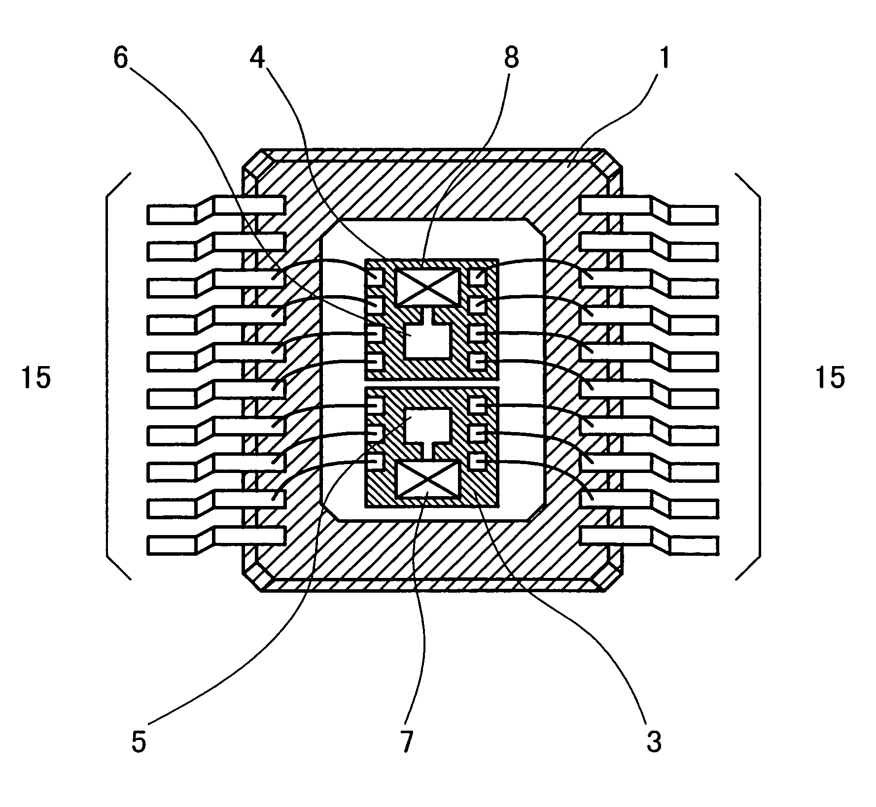
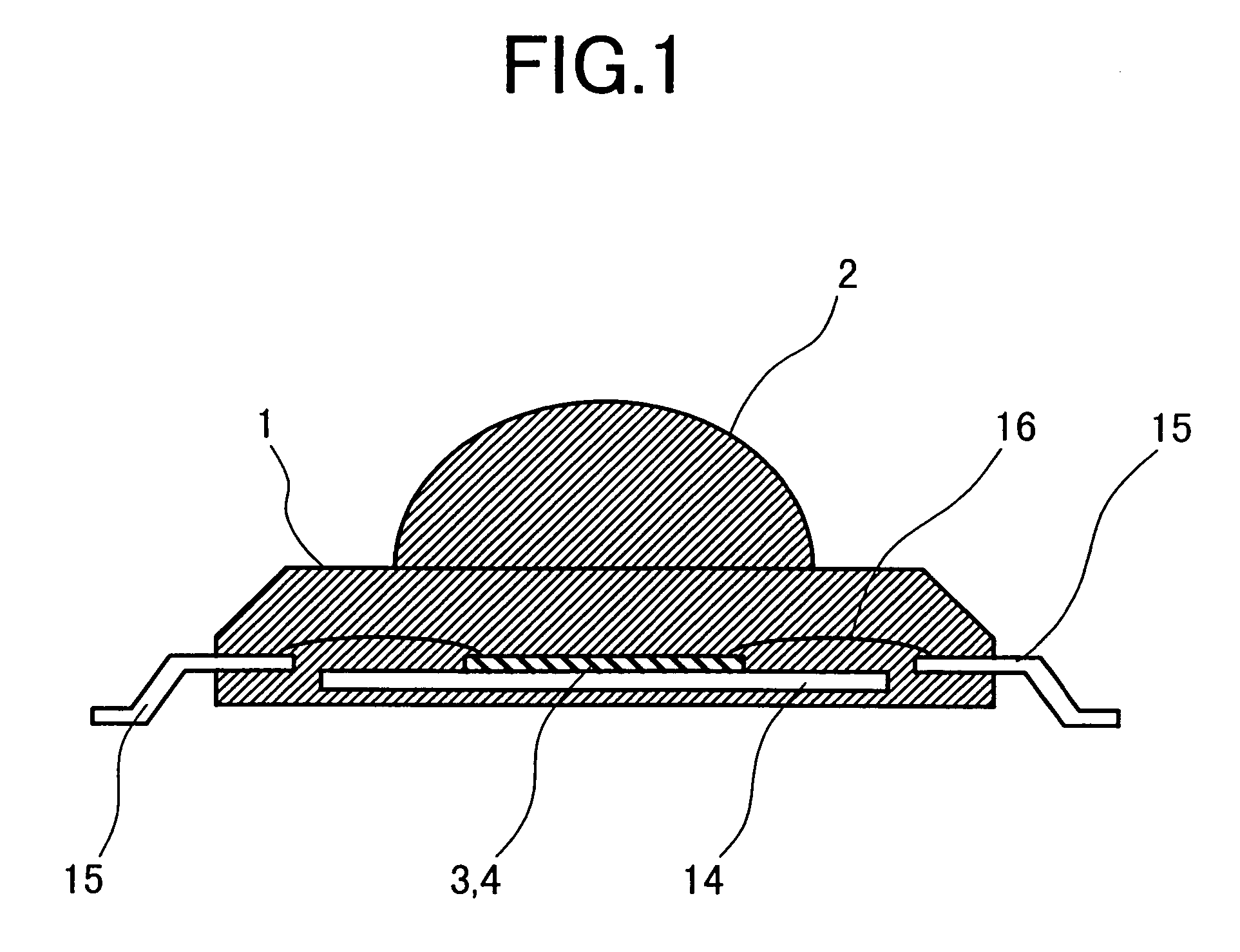
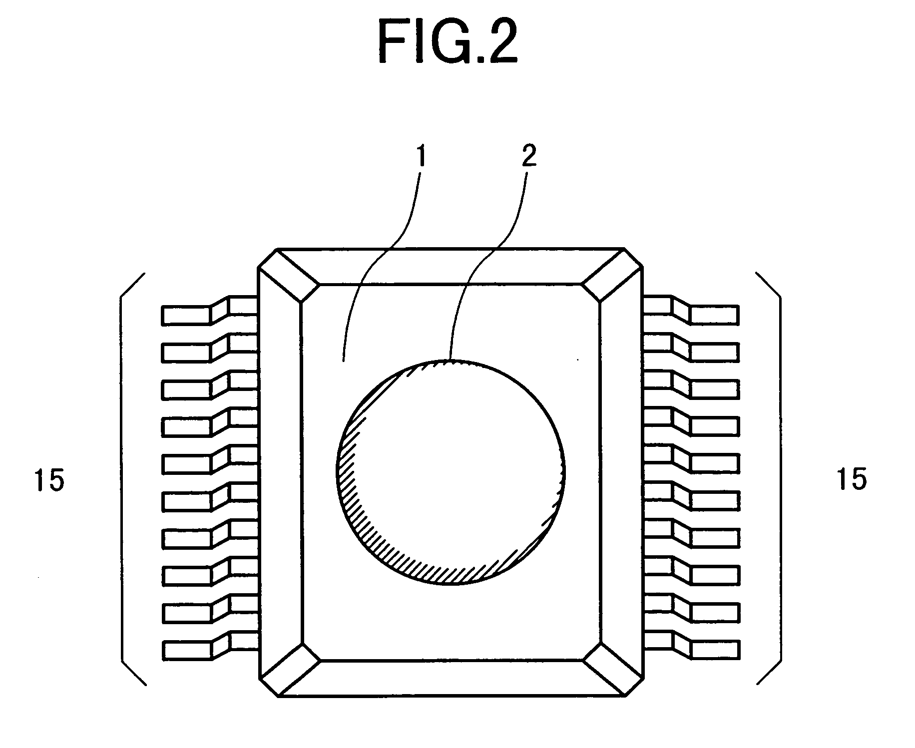
[0031]FIG. 1 through FIG. 3 illustrates the first embodiment of the radar sensor according to the invention. FIG. 1 is a sectional view of the radar sensor; FIG. 2 is a general plan view of the radar sensor; and FIG. 3 is a plan view without the upper part of a package. In this embodiment, a transmission IC3 and a reception IC4 are mounted inside one resin package 1. The transmission IC3 is, as illustrated in FIG. 3, a one-chip MMIC formed on one semiconductor substrate, which includes an active circuit 7 for transmission and a transmission antenna 5. In the same manner, the reception IC4 is a one-chip MMIC formed on one semiconductor substrate, which includes an active circuit 8 for reception and a reception antenna 6. The transmission IC3 and reception IC4 are secured on a base plate 14. The IC3 and IC4 are connected to circuits outside the module through electrode pads o...


PUM


Abstract

The invention intends to provide a sensor module suitable for miniaturization and reduction in costs, in the radar sensor that uses a millimeter or sub-millimeter wave signal of which frequency is more than 20 GHz. To accomplish this problem, the radar sensor is integrated into a one chip MMIC, in which an active circuit including an oscillator and a mixer is formed with an antenna on one semiconductor substrate. Further, the MMIC is sealed with a resin package. A dielectric lens is formed on the resin package over the antenna to attain a desired beamwidth. Thereby, the lens and the resin package can integrally be formed by a metal mold, thus reducing the cost.

Description

[0001]This application is a Continuation application of nonprovisional U.S. Ser. No. 10 / 781,914 filed on Feb. 20, 2000, now U.S. Pat. No. 6,833,806 which is a Continuation of Ser. No. 10 / 227,358 filed on Aug. 26, 2002 now U.S. Pat. No. 6,717,544. Priority is claimed based upon U.S. application Ser. No. 10 / 227,358 filed on Aug. 26, 2002, which claims the priority date of U.S. application Ser. No. 10 / 781,914 filed on Feb. 20, 2004, which claims the priority date of Japanese Patent Application 2002-125910 filed on Apr. 26, 2002.BACKGROUND OF THE INVENTION[0002]1. Field of the Invention[0003]The present invention relates to a radar sensor, more in detail to a receiving unit of radar equipment that radiates a transmission signal and receives a reflection signal from an object having reflected the transmission signal to thereby detect the presence and position of the object, and the moving speed of the object or the vehicle on which the radar is mounted, and so forth, specifically to a ra...

Claims


Application Information

Patent Timeline
Patent Type & Authority Patents(United States)
IPC IPC(8): G01S7/00G01S13/00G01S13/93G01S7/03G01S13/42G01S13/931H01Q1/22H01Q1/32H01Q1/40H01Q1/52H01Q9/04H01Q15/08H01Q19/09H01Q23/00
CPCG01S7/032H01Q1/2283H01Q1/3233H01Q1/40H01Q1/526H01Q9/0407H01Q15/08H01Q19/09H01Q23/00H01L2224/48247G01S13/931H01L2224/48137H01L2224/48091H01L2924/00014H01L2924/181H01L2924/1815H01L2924/00012
Inventor NAGASAKU, TOSHIYUKIKONDOH, HIROSHISHINODA, HIROSHI
Owner HITACHI ASTEMO LTD
Why Eureka
Try Eureka