Direct contact semiconductor cooling

a technology of direct contact and semiconductor, applied in the direction of individual semiconductor device testing, semiconductor/solid-state device testing/measurement, instruments, etc., can solve the problems of undetectable high thermal resistance in applications, reduce the thermal resistance through the semiconductor substrate, and degrade the performance of semiconductor devices, so as to facilitate direct thermal cooling, reduce the thermal spreading resistance, the effect of thermal spreading resistan

Active Publication Date: 2007-01-02
VIASAT INC
View PDF11 Cites 10 Cited by
  • Summary
  • Abstract
  • Description
  • Claims
  • Application Information

AI Technical Summary

Benefits of technology

[0011]In accordance with various aspects of the present invention, thermal spreading resistance, such as that associated with small geometry electronic features that generate heat on a semiconductor, may be reduced through the addition of a thermal transfer fluid. For example, the thermal transfer fluid may be disposed in direct contact with semiconductor heat dissipators. In accordance with an exemplary embodiment, a dielectric fluid may be used within a volume between a semiconductor package and the semiconductor substrate. Therefore, in various exemplary embodiments of the present invention, direct thermal cooling may be employed to reduce the thermal spreading resistance often encountered in MMIC power amplifier devices. In accordance with further embodiments of the present invention, exemplary methods are described herein for sealing a thermal transfer fluid within a volume to facilitate direct thermal cooling.

Problems solved by technology

Excessive temperatures can degrade the performance of semiconductor devices.
This thickness reduction may reduce the thermal resistance through the semiconductor substrate, which often is a poor thermal conductor, e.g. made of silicon or gallium arsenide.
For example, undesirably high thermal resistance exists in applications where heat sources (e.g., transistor gates or channels) have a small geometry relative to the chip, package, and heatsink geometry.
In the case of very small dissipators, e.g., a sub-micron power transistor gate located on the surface of a semiconductor substrate, the spreading resistance may be a significant contributor to undesirably high device temperatures.
Thus, the ability to remove heat from an area near a heat generating device on an integrated circuit continues to be a limiting factor in the performance, reliability, and / or design capabilities of integrated circuit products.

Method used


Image

  • Direct contact semiconductor cooling
  • Direct contact semiconductor cooling
  • Direct contact semiconductor cooling

Examples


Embodiment Construction

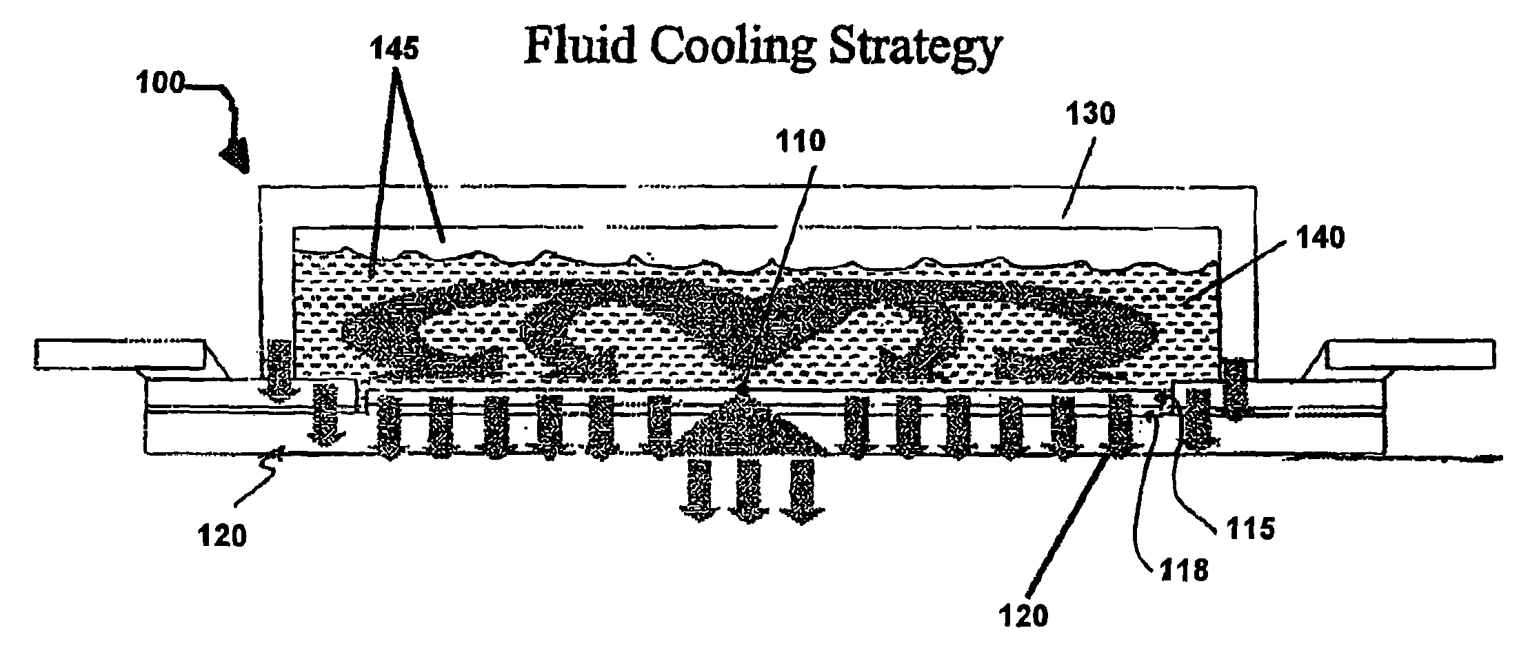
[0016]In accordance with one aspect of the present invention, a semiconductor package may be configured to facilitate the removal of heat from a heat generating source, such as small dissipating electronic feature geometries. In accordance with an exemplary embodiment of the present invention, removal of heat from a heat source is facilitated via conduction and convection through a fluid in contact with the heat source. In accordance with another embodiment of the present invention, use of direct contact fluid cooling systems may reduce thermal spreading resistance.

[0017]As described above, the removal of heat from the local area where it was generated may facilitate enhanced performance of a semiconductor chip. For example, if heat is not removed at sufficient rate, the local temperature may increase enough to cause the chip to fail or to be de-rated or to operate less efficiently. On the other hand, a semiconductor chip having an improved ability to remove heat from the local sour...


PUM


Abstract

Thermal spreading resistance, associated with small geometry electronic features that generate heat on a semiconductor, may be reduced through the addition of a thermally conductive fluid. For example, a dielectric fluid may be used within a volume between a semiconductor package and the semiconductor substrate. Therefore, direct thermal cooling may be employed to reduce the thermal spreading resistance often encountered in MMIC power amplifier devices. Furthermore, exemplary methods to achieve this sealing are described herein.

Description

CROSS REFERENCE TO RELATED APPLICATIONS [0001]This application claims the benefit of, and priority to, provisional application Ser. No. 60 / 481,630, filed Nov. 12, 2003, which application is hereby incorporated by reference in its entirety.FIELD OF THE INVENTION [0002]The present invention generally relates to systems and methods for enhancing the cooling of a semiconductor chip at the circuit level. More particularly, the present invention relates to direct contact semiconductor cooling of heat dissipating electronic features on semiconductor devices, such as those having small geometries.BACKGROUND OF THE INVENTION [0003]Excessive temperatures can degrade the performance of semiconductor devices. As an example, in an integrated circuit (“I”) chip, heat is generally generated through the operation of various integrated circuit devices on the chip. The heat from the individual IC devices is often conducted away from the IC devices to a heatsink. In a typical Personal Computer, heat f...

Claims


Application Information

Patent Timeline
Patent Type & Authority Patents(United States)
IPC IPC(8): H01L23/34G01R31/26H01L23/24H01L23/44
CPCH01L23/44H01L2224/48091H01L2924/1305H01L2924/00014H01L2924/00
Inventor TORKINGTON, RICHARD S.FILREIS, JONBUER, KENNETH V.
Owner VIASAT INC
Why Eureka
Try Eureka