Method of forming shallow doped junctions having a variable profile gradation of dopants

a technology of dopant and profile, applied in the field of manufacturing integrated circuits, can solve the problems of draining power through the integrated circuit, undesirable increase of reverse bias current leakage, and the process used to produce shallow junctions still exhibit certain problems, so as to reduce the depth of the dopant implanted, eliminate reverse bias current leakage, and low resistance

Inactive Publication Date: 2007-02-20
ROUND ROCK RES LLC
View PDF12 Cites 26 Cited by
  • Summary
  • Abstract
  • Description
  • Claims
  • Application Information

AI Technical Summary

Benefits of technology

[0016]The present invention also relates to a method which remedies rough and jagged unevenness of the bottom component of the junctions, abrupt dopant concentration gradient termination of the junctions, and high reverse bias current leakage which results from PLAD formation of junctions.
[0021]The semiconductor wafer is then annealed. The anneal causes a more even distribution of dopant concentration therein and helps to remove imperfections in the internal lattice structure. This anneal is optional and can be conducted after each doping operation, or after any of the doping operations.
[0022]The doping operation which forms a heavily doped inner portion and the doping operation which forms a lightly doped outer portion can be conducted in reverse order. This is useful in forming a thin oxide layer over the surface. One application for the thin oxide layer is as an implant barrier to the PLAD operation. When using an implant barrier, a conventional ion bombardment implantation doping operation is conducted first, and then the thin oxide layer is deposited using a process that forms the oxide layer, such as a tetraethyl orthosilicate (TEOS) layer. The PLAD operation is then conducted through the thin oxide layer. Thus, the lightly doped outer portion is formed without the existence of the thin oxide layer, while the thin oxide layer is present to serve as an implant barrier to the PLAD operation. This use of a thin oxide layer as an implant barrier in this embodiment further reduces the depth of the dopants implanted in the PLAD operation, while maintaining the depth of the dopants implanted by the conventional ion bombardment implantation doping operation. The use of a thin oxide layer as an implant barrier also maintains the high concentration of dopants on the surface of the shallow junction in order to form a low resistance contact and interconnect interface.
[0023]The result of the method of the present invention is a shallow junction which is useful for forming diodes, resistors, and transistors. The junction has a variable profile gradation of dopants, with a first concentration of dopants in a heavily doped inner portion, and a second, lower concentration of dopants in the deeper lightly doped outer portion. The junction is also formed with an even bottom edge which, along with the variable profile gradation of dopants, helps to eliminate reverse bias current leakage. The variable profile gradation of dopants also helps to reduce underlap, and thereby helps to maintain a low threshold voltage without the need for forming spacers.
[0024]The method of the present invention has been found to be easily integrated into the manufacturing flow process and to be relatively inexpensive.

Problems solved by technology

Nevertheless, the PLAD processes used to produce shallow junctions still exhibit certain problems.
The abrupt dopant concentration gradient termination, together with unevenness of bottom component 16a, cause an undesirable increase in reverse bias current leakage.
Reverse bias current leakage causes a drain of power through the integrated circuit when finished, a problem which is at odds with the low power requirements of modern integrated circuit applications.
A high threshold voltage is generally undesirable in MOS transistors.
Nevertheless, the use of spacers 18 does not solve the problems of reverse bias current leakage.

Method used


Image

  • Method of forming shallow doped junctions having a variable profile gradation of dopants
  • Method of forming shallow doped junctions having a variable profile gradation of dopants
  • Method of forming shallow doped junctions having a variable profile gradation of dopants

Examples


Embodiment Construction

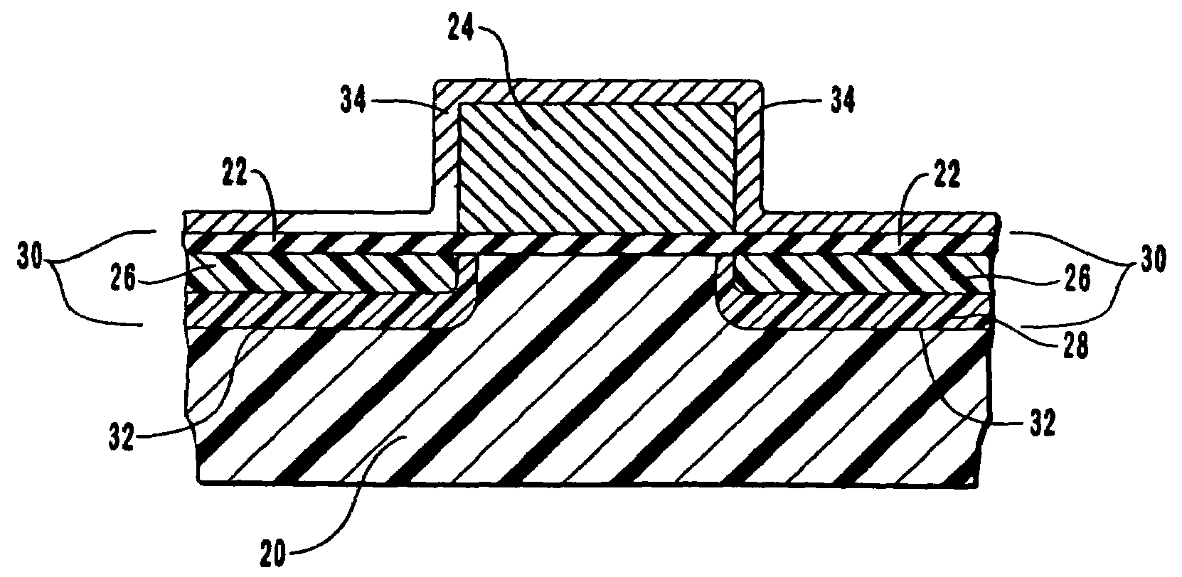
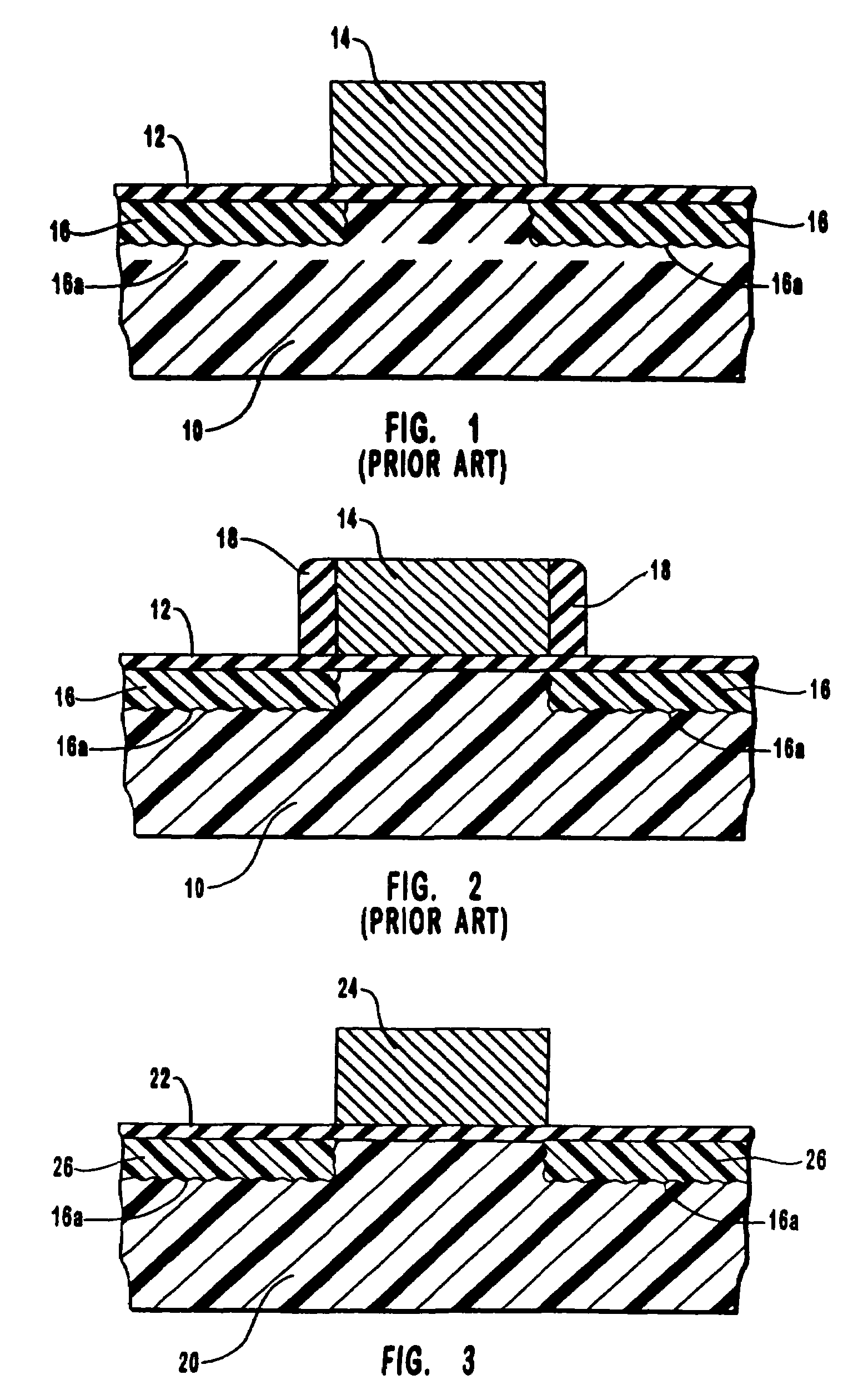
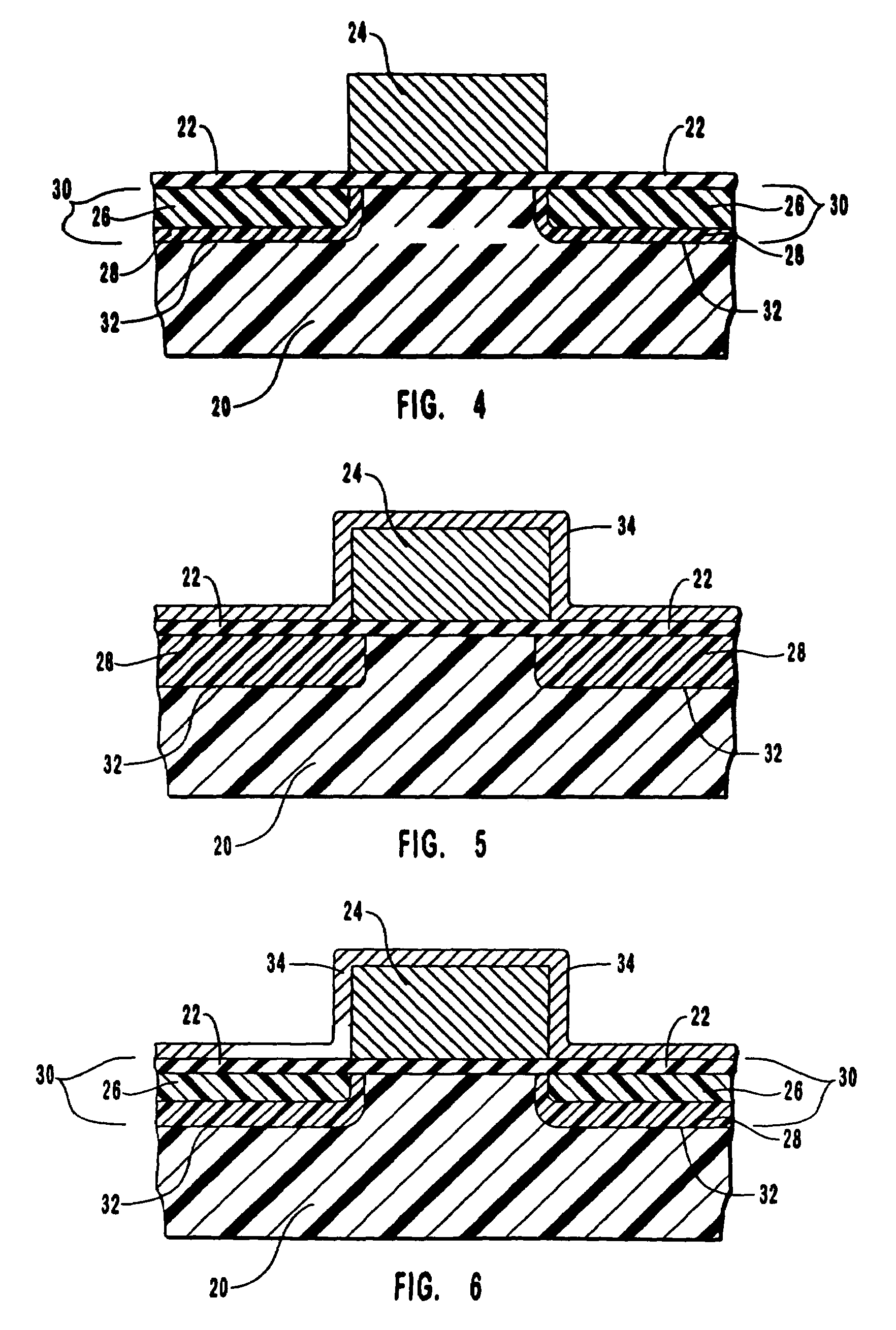
[0033]The present invention involves the discovery by the inventors that by creating a shallow junction that has a variable concentration profile gradation of dopants with a PLAD operation, the prior art problems of conventional PLAD processes of jagged unevenness of the bottom component of the junction, excessive underlap of junctions below a MOS gate due to out diffusion of dopants, and reverse bias current leakage can be remedied. Thus, the present invention comprises a method of forming a shallow junction on a silicon substrate using PLAD, which results in a junction with a variable concentration profile gradation of dopants for the formation of a less abrupt dopant concentration gradient termination at the bottom component of the junction. The term “variable concentration profile gradation of dopants,” as used herein, refers to a junction in which different depths of the junction have different concentrations of dopants. Thus, the shallow junction has differing concentrations t...


PUM


Abstract

Disclosed are methods for forming a shallow junction with a variable concentration profile gradation of dopants. The process of the present invention includes first providing and masking a surface on an in-process integrated circuit wafer on which the shallow junction is to be formed. Next, a low ion velocity and low energy ion bombardment plasma doping or PLAD operation is conducted to provide a highly doped inner portion of a shallow junction. In a further step, a higher ion velocity and energy conventional ion bombardment implantation doping operation is conducted using a medium power implanter to extend the shallow junction boundaries with a lightly doped outer portion. In various embodiments, the doping steps can be performed in reverse order. In addition, an anneal step can be performed after any doping operation.

Description

CROSS-REFERENCE TO RELATED APPLICATIONS[0001]This application is a divisional of application Ser. No. 10 / 804,578, filed Mar. 19, 2004, now U.S. Pat. No. 7,060,599, which is a continuation of application Ser. No. 09 / 981,549, filed Oct. 17, 2001, now U.S. Pat. No. 6,717,211, issued Apr. 6, 2004, which is a continuation of application Ser. No. 09 / 196,515, filed on Nov. 20, 1998, now U.S. Pat. No. 6,359,310, issued Mar. 19, 2002, which is a continuation of application Ser. No. 08 / 654,573, filed on May 29, 1996, now abandoned, each of the foregoing being incorporated herein by reference in their entirety.FIELD OF THE INVENTION[0002]The present invention is directed to the manufacture of integrated circuits. More particularly, the present invention is directed to shallow junctions formed on in-process integrated circuit wafers and to methods of forming the shallow junctions using plasma doping.BACKGROUND OF THE INVENTION[0003]The semiconductor industry is in the midst of a movement toward...

Claims


Application Information

Patent Timeline
Patent Type & Authority Patents(United States)
IPC IPC(8): H01L21/8238H01L21/223H01L21/265H01L21/336H01L29/78
CPCH01L21/2236H01L21/26513H01L21/2652H01L29/6659H01L29/7833H01L29/7836Y10S257/90H01L29/66575
Inventor GONZALEZ, FERNANDOTHAKUR, RANDHIR
Owner ROUND ROCK RES LLC
Why Eureka
Try Eureka