

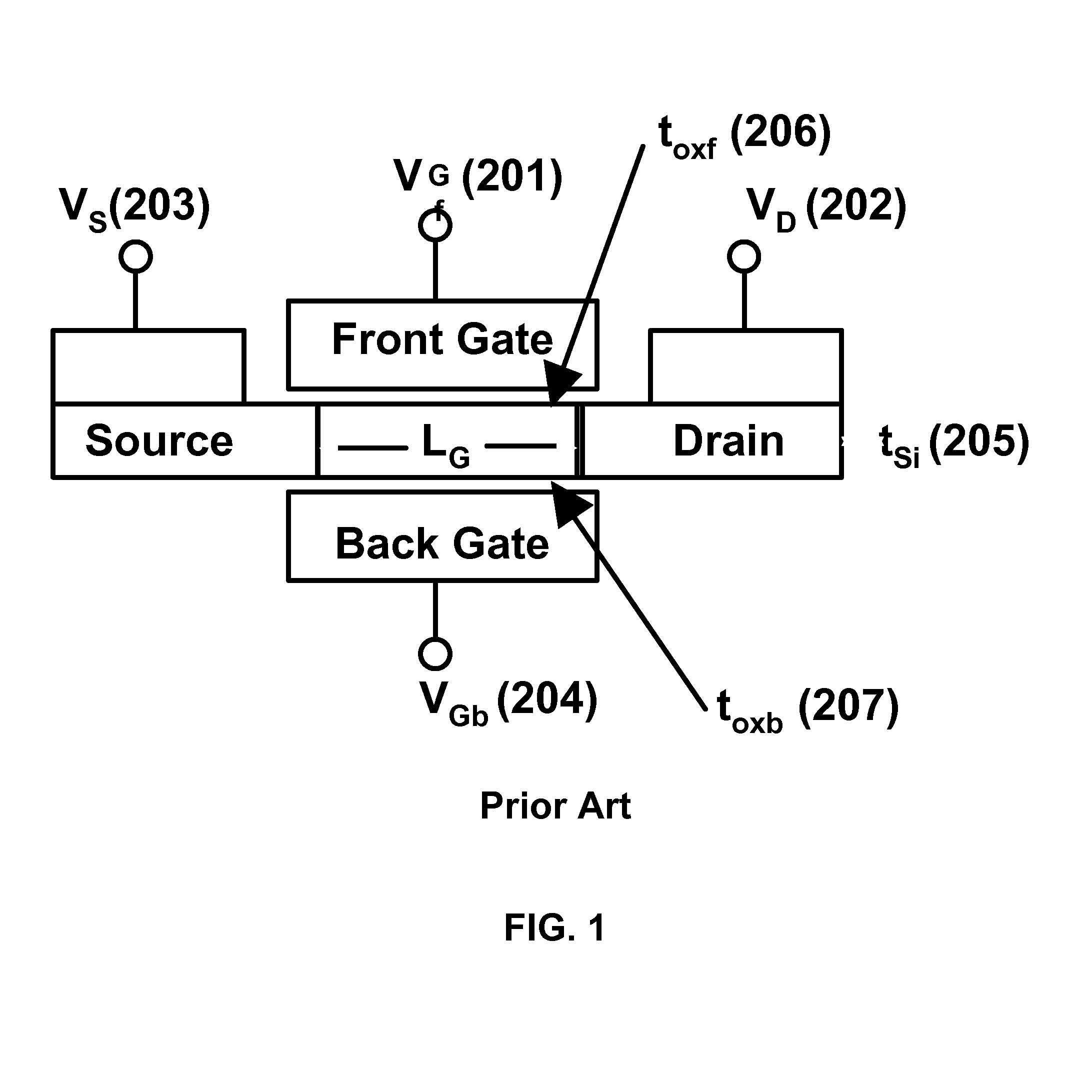
Double gate (DG) SOI ratioed logic with intrinsically on symmetric DG-MOSFET load
- Summary
- Abstract
- Description
- Claims
- Application Information
AI Technical Summary
Benefits of technology
Problems solved by technology
Method used
Image

Examples
Embodiment Construction
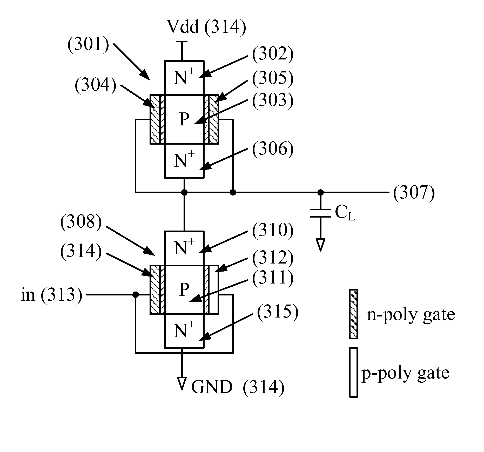
[0034]The present invention is an SOI Logic family composed of an intrinsically on symmetric fully depleted double gate MOSFET load and an asymmetric fully depleted double gate MOSFETs as the drivers.
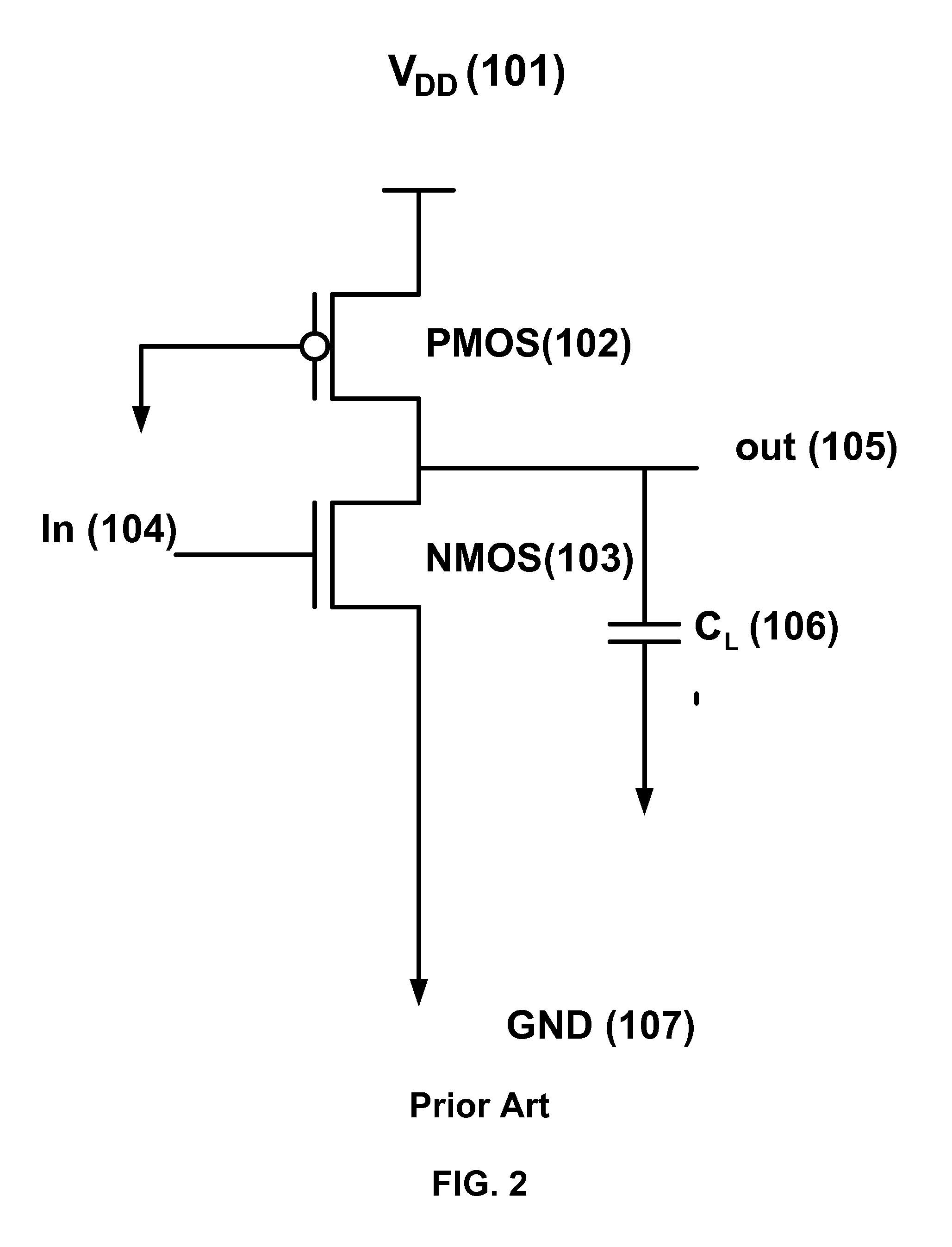
[0035]This invention may provide a high speed low power logic family for double gate SOI technology. The basic element of the digital circuit is the digital inverter, which provides a digital output signal that is the digital complement of the input. For example, if the input is “HIGH,” then the output is “LOW,” and vice versa. There are certain parameters for a digital inverter that may make it more robust and a better design. The parameters includes a noise margin, which should be high, a threshold voltage, and load current characteristics vs. output voltage.
[0036]A best mode practice for the ratioed SOI inverter with FD symmetric DG-MOSFET load will now be explained. Referring to FIG. 3, we see an illustrative example of the present invention. Load transistor 301 is a double gate NMO...
PUM
 Abstract
Description
Claims
Application Information