

Magnetic recording medium
a magnetic recording and recording medium technology, applied in the field of magnetic recording mediums, can solve the problem that the grain size of the magnetic grains in the magnetic layer cannot be controlled withou
- Summary
- Abstract
- Description
- Claims
- Application Information
AI Technical Summary
Benefits of technology
Problems solved by technology
Method used
Image

Examples
example 1
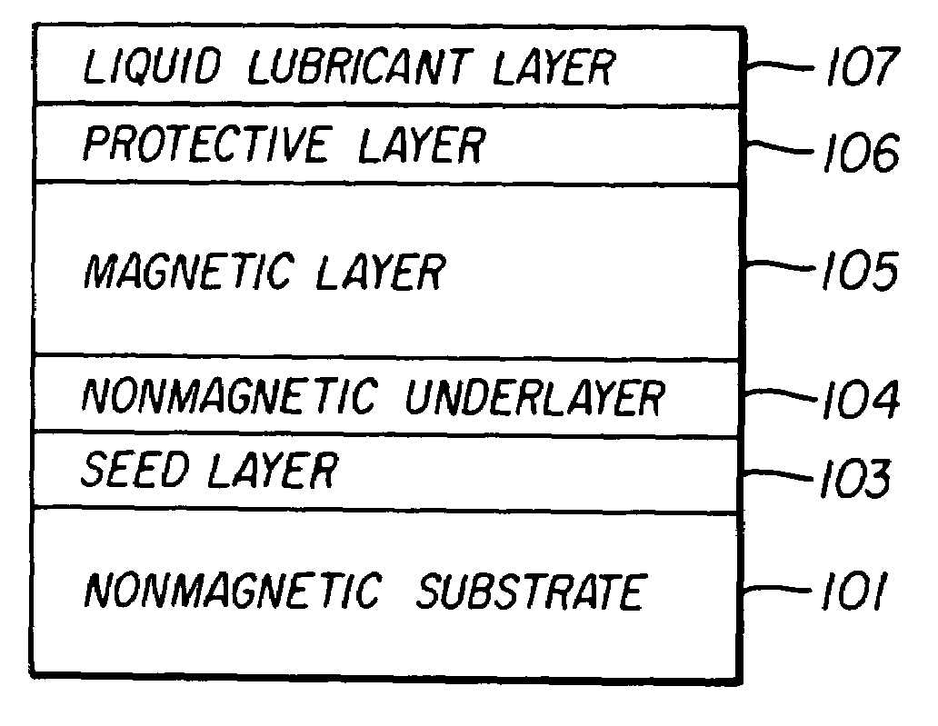
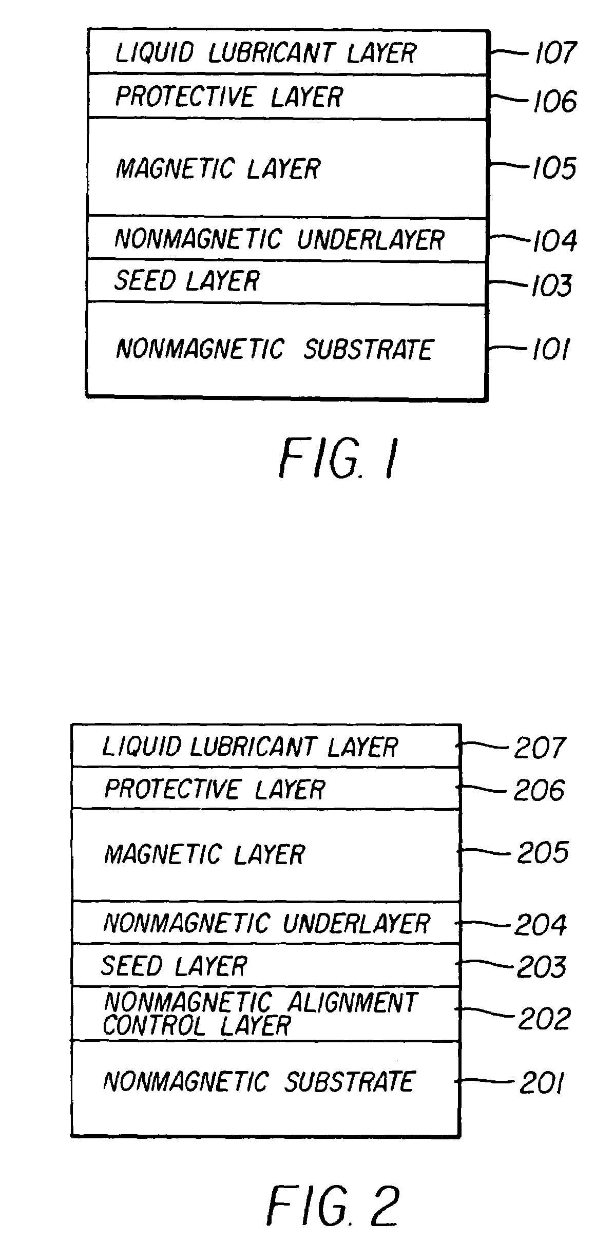
[0042]A resin substrate of 3.5″ diameter disk was used for a nonmagnetic substrate. After cleaning, the substrate was introduced into a sputtering apparatus. A nonmagnetic alignment control layer of amorphous NiP 5 nm thick was deposited under the argon gas pressure of 5 mTorr. After forming a seed layer of platinum with the 5 nm thickness, a nonmagnetic underlayer 20 nm thick was deposited at the rate of 2.3 nm / sec under the discharging argon gas pressure of 30 mTorr. The nonmagnetic underlayer was formed using a titanium alloy containing 10 at % of Cr, Ta, Re, or Ru. Subsequently, a granular magnetic layer 30 nm thick was formed by an RF sputtering method using a target of Co76Cr12Pt12 containing 10 mol % of SiO2 under the discharging argon gas pressure of 5 mTorr.
[0043]After laminating a carbon protective layer 8 nm thick, the laminated substrate was taken out from the vacuum chamber. Finally, liquid lubricant was applied to form a liquid lubricant layer 1.5 nm thick. Thus, a mag...
example 2
[0047]A medium of Example 2 was produced in the same manner as in Example 1 except that a nonmagnetic underlayer is comprised of ruthenium and no layer was deposited over the underlayer. A nonmagnetic underlayer 20 nm thick was formed by means of a sputtering method at the deposition rate of 4.2 nm / sec under a discharging argon gas pressure of 70 mTorr. Transmission electron microscope (TEM) observation of the cross section of the produced medium revealed columnar crystals and porous structure in the direction vertical to the substrate. The columnar crystals were observed grown without extraordinary growth such as abnormal expansion during the growth process.
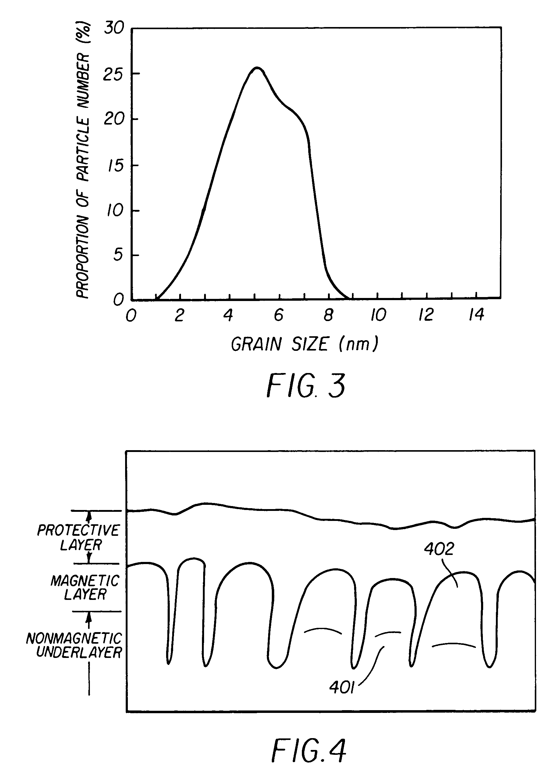
[0048]Initial stage of the deposition process did not generate an “initial growth layer”. Planar observation was done by the TEM to measure grain sizes. Average grain size was about 6 nm. The distribution of the grain sizes was a normal distribution and the standard deviation was 1.8 nm. Here, the standard deviation in this appl...
example 3
[0051]A medium of Example 3 was produced in the same manner as in Example 2 excluding the deposition process of the nonmagnetic underlayer.
[0052]Each of nonmagnetic underlayers of ruthenium was deposited to various thicknesses by a sputtering method at the deposition rate of 4.2 nm / sec under discharging argon gas pressure of 70 mTorr. Grain sizes were measured by a planar image analysis using the TEM for the underlayers with the thicknesses of 5 nm and 50 nm resulting in the average grain sizes of 5 nm and 8 nm, respectively. The both distributions of grain sizes were normal distributions with the standard deviations of 1.4 nm and 2.2 nm, respectively. The cross sectional structure of the both films showed columnar structure and no initial growth layer.
[0053]Deposition was conducted under the argon gas pressures of 1.2 times, and 0.7 times above value of 70 mTorr, at the fixed deposition rate of 2.3 nm / sec and with the fixed film thickness of 20 nm. Grain size analysis was made on t...
PUM
 Abstract
Description
Claims
Application Information