Method of reducing the pattern effect in the CMP process

a technology of pattern effect and cmp, which is applied in the direction of semiconductor/solid-state device manufacturing, basic electric elements, electric apparatus, etc., can solve the problems of unsatisfactory pattern effect, dishing phenomenon, and deterioration of electrical properties, so as to reduce dishing phenomenon, improve the end-point detecting function of the polishing machine, and prolong the transition stage. the effect of tim

Inactive Publication Date: 2007-02-27
TAIWAN SEMICON MFG CO LTD
View PDF4 Cites 11 Cited by
  • Summary
  • Abstract
  • Description
  • Claims
  • Application Information

AI Technical Summary

Benefits of technology

[0014]An advantage of the present invention is that, by removing part of the conductive layer in the CMP process and re-depositing the conductive layer, the duration time of transition stage is increased, this in turn improves the end-point detecting function of the polishing machine and can effectively reduce the dishing phenomenon caused by the pattern effect in the CMP process, and the RS is improved.
[0015]According to the feature of the present invention, the method of eliminating the dishing phenomena after a CMP process comprises the steps of providing a semiconductor substrate having a patterned dielectric layer, a barrier layer over the patterned dielectric layer, and a conductive layer over the barrier layer; performing a first CMP process to a polishing end point to remove part of the conductive layer, wherein the dishing phenomena occur on the conductive layer; depositing a layer of material substantially the same as the conductive layer over the conductive layer; and performing a second CMP process to expose the patterned dielectric layer.
[0016]According to the feature of the present invention, the CMP rework method comprises the steps of providing a semiconductor substrate which is reported by a CMP machine as an abnormally polished wafer at a predetermined CMP end point and has a patterned dielectric layer, a barrier layer over the patterned dielectric layer, and a conductive layer over the barrier layer; depositing a layer of material substantially the same as the conductive layer over the conductive layer; and performing a CMP process to expose the patterned dielectric layer. The CMP rework method of the present invention can resolve the problems of serious dishing phenomena, sheet resistance variations, and low yields accompanied by conventional CMP rework methods.

Problems solved by technology

However, during the CMP process, if an area ratio of the conductive wire to the insulating layer is too large, a pattern effect arises, resulting in the phenomenon known as “dishing”.
As the dishing phenomenon occurs, sheet resistance (RS) varies, and as a result the electrical properties deteriorate.
Therefore, the pattern effect is undesirable.
The substrate, however, is often at the dishing stage, as shown in FIG. 2d, and exhibits a serious dishing phenomenon caused by the pattern effect.
Furthermore, the end-point for polishing is often erroneously reached due to faulty signal collection.
Generally, more than 20% polished wafers have end-point failure and become abnormal substrates reported by CMP machines.
The conductive layer (for example, Cu) thickness is often incorrectly reported due to the narrow operating window, which results from the very short transition stage.
This leads to additional complications in maintaining the desired metal topography and requires CMP rework for failed wafers.
It is difficult, however, to find an adequate recipe to rework wafers because the under-polish levels of polished wafers are event-related.
In addition, the problems of the dishing phenomena caused by over polishing after a CMP process and the abnormal wafers reported by CMP machines need to be solved.
The copper layer is deposited to fill the trench at a level approaching the top surface of the underlying wafer, but not overfill the trench, and the deposition of copper alloy comprising metal other than copper increases the process complexity.

Method used


Image

  • Method of reducing the pattern effect in the CMP process
  • Method of reducing the pattern effect in the CMP process
  • Method of reducing the pattern effect in the CMP process

Examples


example

Example 1

The Method of Reducing the Pattern Effect in the CMP Process According to the Present Invention

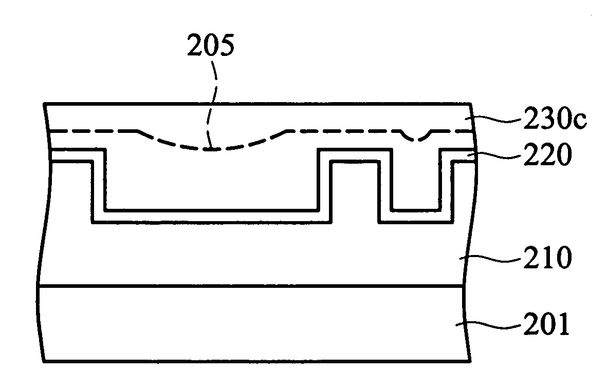
[0046]The example was performed using the method of reducing the pattern effect in the CMP process of the present invention mentioned above, wherein silicon dioxide was used as the patterned dielectric layer with trench patterns of squares (110×110 μm2) and isolated lines (5×350 μm2), TiN was used to form the barrier layer with a thickness of 250 ű50 Å, a copper layer was deposited as a conductive layer by copper seeding and then electrochemical plating on the TiN barrier layer and had a thickness of 6000 ű600 Å and average step heights of about 4900 Å for the square area and about 1500 Å for the isolated line area.

[0047]After the first CMP process was performed, the thickness of the remaining copper layer higher than the TiN barrier layer was about 4800 ű480 Šand was approximately planar. Copper was re-deposited on the remaining copper layer by electrochemical plating to for...

example 2

The Method of Eliminating the Dishing Phenomena after a CMP Process According to the Present Invention

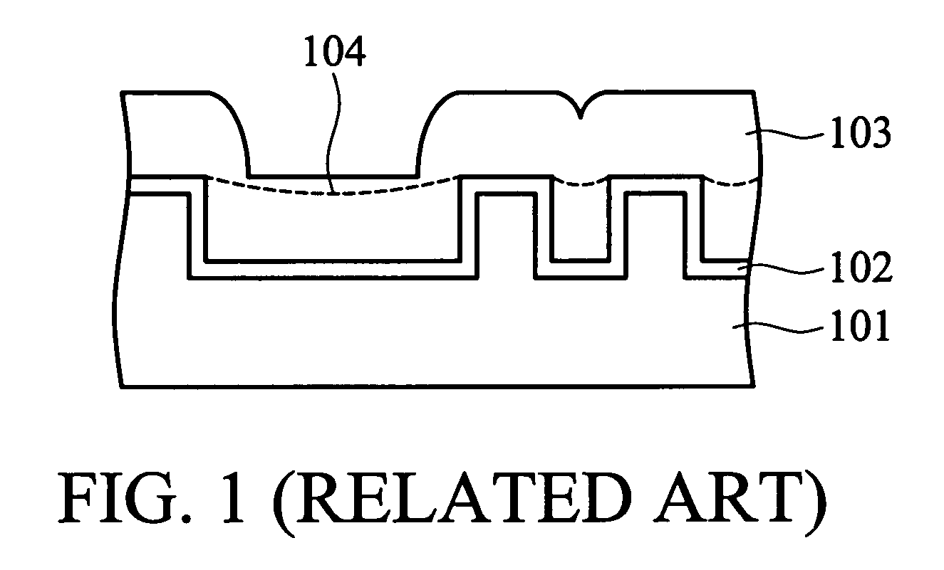
[0051]A semiconductor substrate with dishing phenomena after a CMP process was provided. The semiconductor substrate contained a patterned dielectric layer, a TiN barrier layer with a thickness of 250 ű50 Å, an end-point-polished copper layer with a dishing depth of about 1200 Å at the trench pattern. A layer of copper was electrochemically plated on the polished copper layer, resulting a copper layer with a total thickness (from the top surface of the barrier layer to the top surface of the copper layer) of about 6000 Å. Then, a CMP process was performed. At the end of the CMP process, a planar surface of the copper layer was obtained.


PUM

PropertyMeasurementUnit
conductiveaaaaaaaaaa
area ratioaaaaaaaaaa
sheet resistanceaaaaaaaaaa

Abstract

A method of reducing the pattern effect in the CMP process. The method comprises the steps of providing a semiconductor substrate having a patterned dielectric layer, a barrier layer on the patterned dielectric layer, and a conductive layer on the barrier layer; performing a first CMP process to remove part of the conductive layer before the barrier layer is polished, thereby a step height of the conductive layer is reduced; depositing a layer of material substantially the same as the conductive layer on the conductive layer; and performing a second CMP process to expose the dielectric layer. A method of eliminating the dishing phenomena after a CMP process and a CMP rework method are also provided.

Description

BACKGROUND OF THE INVENTION[0001]1. Field of the Invention[0002]The present invention relates in general to a chemical mechanical polishing (CMP) process in semiconductor manufacturing. In particular, the present invention relates to a method of reducing the pattern effect in a CMP process, a method of eliminating the dishing phenomena after a CMP process, and a CMP rework method.[0003]2. Description of the Related Art[0004]Chemical mechanical polishing (CMP) has been popularly applied to the planarization treatment of conductive wires in logic device processing and contact window processing, and especially, to the fabrication of sub-130 nm interconnects in ultra-large scale integration (ULSI) silicon device. With respect to a damascene technique, the desired process requires removal of the metal (such as copper) overburden followed by the over-polishing to ensure that all residual copper is completely removed. However, during the CMP process, if an area ratio of the conductive wire...

Claims


Application Information

Patent Timeline
Patent Type & Authority Patents(United States)
IPC IPC(8): H01L21/4763H01L21/302H01L21/321H01L21/44H01L21/768
CPCH01L21/7684H01L21/3212
Inventor LIU, CHI-WENTSAO, JUNG-CHIHFENG, SHIEN-PINGCHEN, KEI-WEILIN, SHIH-CHICHUANG, RAY
Owner TAIWAN SEMICON MFG CO LTD
Why Eureka
Try Eureka