
Universal hardware device and method and tools for use therewith

a hardware device and universal technology, applied in the field of circuit design and testing and device architecture, can solve the problems of long development cycle, high cost, long time required to market integrated circuits, etc., and achieve the effect of facilitating design and simulation of devices and reducing the time from design to marketing

Inactive Publication Date: 2007-02-27
OFER MEGED
View PDF31 Cites 40 Cited by
  • Summary
  • Abstract
  • Description
  • Claims
  • Application Information

AI Technical Summary

Benefits of technology

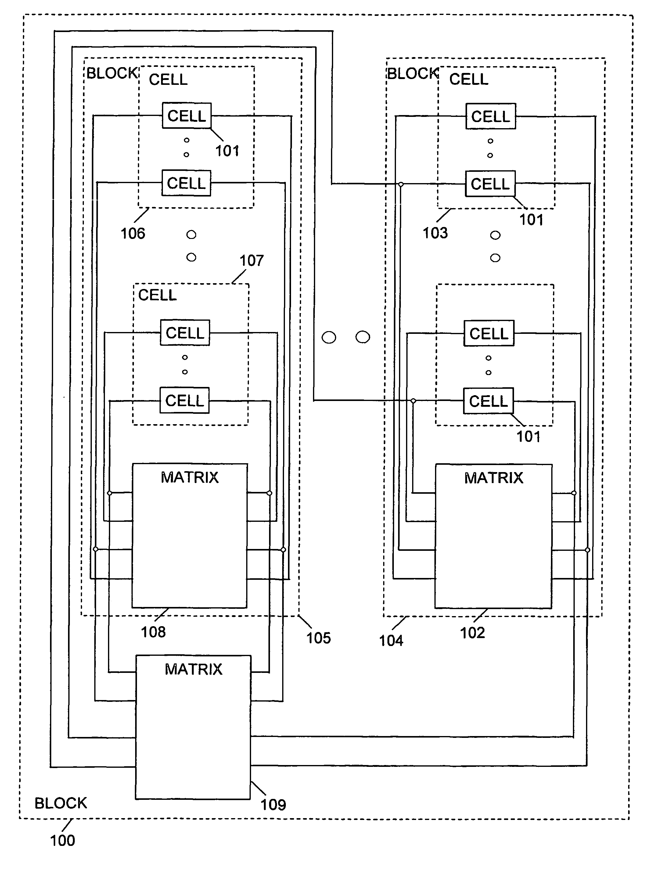
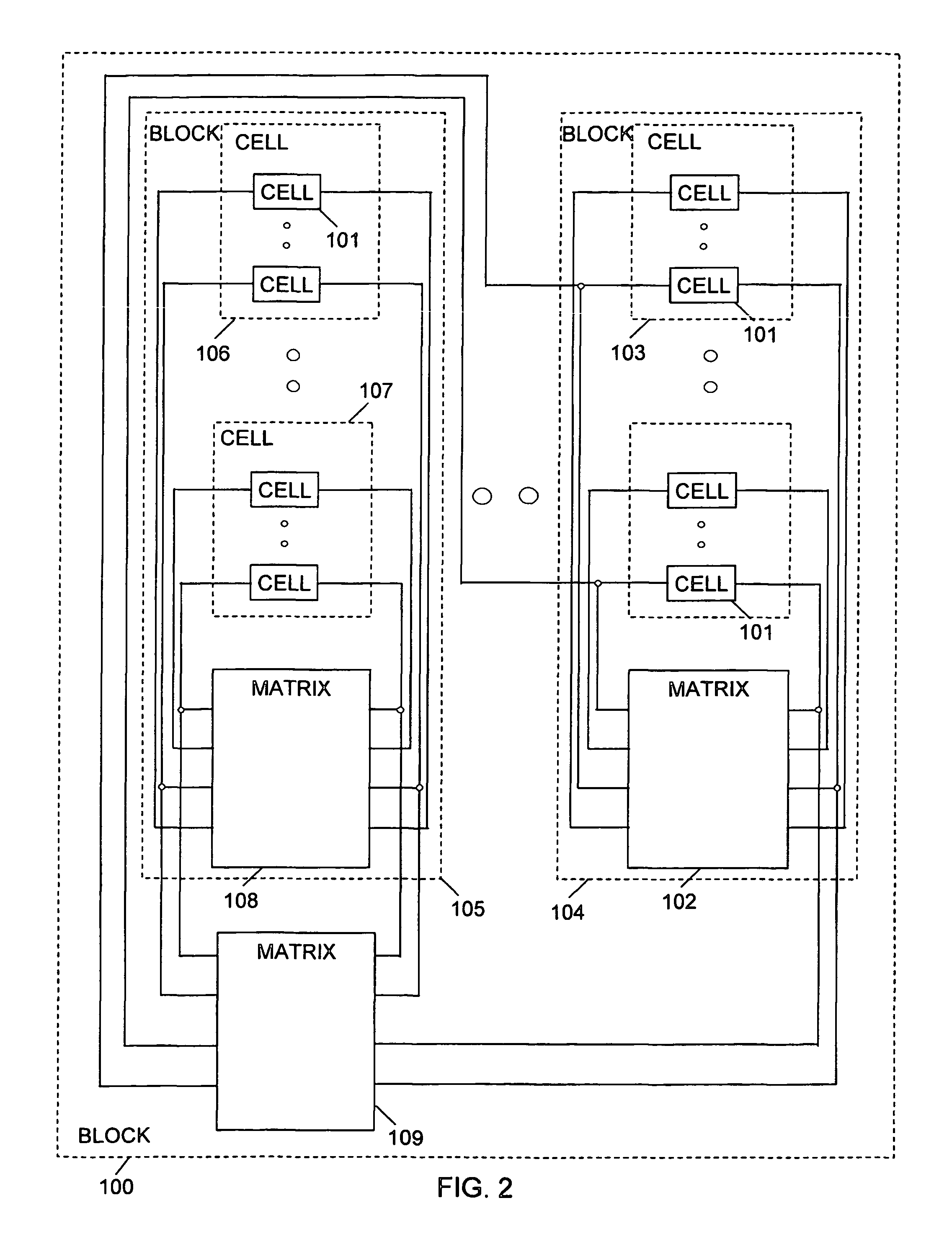
"The invention is a device architecture that allows for the flexible design of digital circuits, reducing the time from design to finished product. It consists of cells for storing data and a programmable matrix for connecting the cells. The cells can be combined to form larger cells, which can be programmed for different functions and used as hardware applications. The device operates independently of the efficiency of the high-level program code used to implement the functions. The invention also provides tools for designing, simulating, and debugging the device, assisting in converting it to an ASIC."

Problems solved by technology

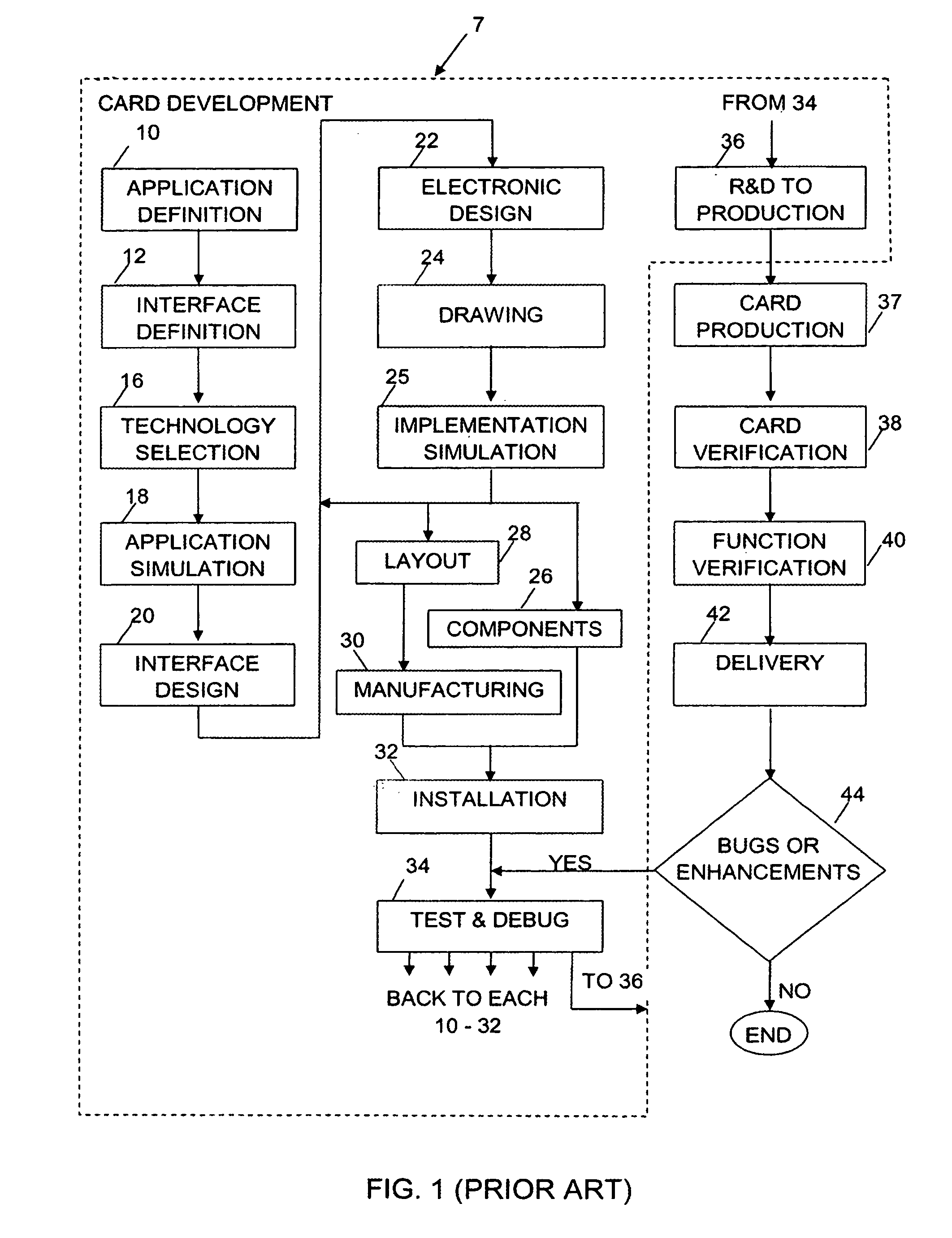
Known design and manufacturing processes of integrated circuits (ICs) and modules containing ICs including implementation using DSPs or Application Specific Integrated Circuits (ASIC) require lengthy development cycles and are expensive.
In particular, the time required to market integrated circuits is long owing to the length of the development period requiring protracted design, verification and testing of the application.
During verification and testing of the product, failures in the design may be detected requiring debugging and repair, this greatly adds to the development cost and time, particularly when design failures are detected at the end of the process, for example after product delivery.
Hardware products are expensive since the time to market influences engineering costs, market loss, and so on.
Costs must also bear the overhead of testing equipment used during development, the expense of testing equipment used during manufacturing, inventory size and the costs relating to employment of professional engineers.
Simulation accuracy is poor.
If simulation of high-resolution delays is required, simulation becomes cumbersome.
Moreover, simulations are very slow, often hundreds of thousands times slower than real-time.
Yet another drawback of known design and development processes is that the size of prototypes and non-ASIC electronic cards may exceed practical dimensions.
The ability to test high-end System on a Chip products is limited owing to the very high density of integrated circuits, making it very difficult to probe points of interest in the circuit.
It is likewise difficult to test finished products containing high-density integrated circuits, and to verify the complete functionality of complex circuits.
The adaptation of already designed products to advanced chip production technologies so as to ensure the compatibility of applications to newer technologies, is poor.
This impacts not only on the application developer but also makes it difficult for the chip manufacturer to employ new geometries whilst enabling developers to use their existing applications.
This is a time-consuming and expensive process.
Typically, application speed is enhanced by implementing the application in hardware at then expense of functional flexibility since most hardware implementations are dedicated to a specific application and are not amenable to extension or changes.
Yet another drawback associated with the industry is the relative scarcity of qualified personnel and the difficulty in breaking down the design and development so as to be amenable to sharing amongst several engineers in order that the development cycle may be reduced.
All these limitations combine to increase both the length and the cost of the development and manufacturing cycle.
Hardware implementation is the fastest (real-time) solution, but it can do only a limited number of tasks, is not flexible and is large.
Time to market is lengthy.
The development and manufacturing processes are expensive.
In practice, ASIC conversion suffers from all the problems mentioned above.
The electronic design process is complicated, as the engineer has to remember a lot of different components and the way to use them.
The more complicated the application, the more time is needed for the design.
The more complicated the application, the more time is needed for the drawings.
It sometimes takes quite a long time to purchase a specific device, thereby delaying prototype production.
The more complex the application, the more components are used, the longer is the time to production and the bigger is the inventory of components.
The more complex the application, the more components are used and the longer the layout time.
For each application a different board must be manufactured thus increasing the amount of human resources invested and the need for expensive equipment for card verification and manufacture.
Faults in the layout can cause problems in the installation.
Specifically, installation in the development phase uses less automation and the probability of a faulty card is greater.
To shorten the installation period, special purpose, expensive equipment is used, for example high pitch chip insertion equipment.
Verification is quickly becoming the biggest technology barrier.
Errors can be made in each one of the above tasks.
For example, narrow spacing between tracks of a printed circuit can cause a short circuit.
It is worse if this kind of mistake is not discovered in the debugging process, because it may be found later when it is more expensive to repair.
That means repetitive processes occur.
The above process causes the development and manufacturing cycle to be long.
The later an error is found the harder and the more expensive is the repair.
Therefore, if an ASIC is needed, considerable effort is made to assure error-free results.
It is quite complicated and time consuming to create automatic equipment for testing each function of the application.
If an error is found or an enhancement is needed at the end of the process, repairs and enhancements 44 are very difficult, expensive and time consuming.
This solution is slower in real-time than an equivalent hardware implementation.
The DSP implementation is about the same size as the hardware implementation, but generally DSP implementations do not allow the option of conversion into ASIC.
Although the above-described hardware development process must also be implemented for the DSP card, it rarely influences the time to market period for several reasons.
This conversion process influences the cost as well as the time to market.
In practice, there is no efficient means of conversion from the simulation to the DSP code.
In other words, the simulation does not simulate the exact implementation, especially if assembly language is used in the DSP coding.
Also, the cost of R&D is high.
The market is short of DSP experts so the wages expense is high.
In production, automatic function verification is still hard to implement, but if an error or enhancement is discovered after delivery, it still can be fixed by changing the software at the customer's premises, although in practice this is far from trivial.
Programmable Logic Devices (PLDs) allow for flexible implementation but are limited in the application capability for a given chip area.
Simulation is not accurate, debugging is complicated and the product is expensive.
In this case, it is common to have a few iterations for the ASIC development, which increases price and time to market.

Method used


Image

  • Universal hardware device and method and tools for use therewith
  • Universal hardware device and method and tools for use therewith
  • Universal hardware device and method and tools for use therewith

Examples


example 1

Counter

[0138]FIG. 10 shows schematically a counter 160 using one cell 110 comprising a RAM 111 having an n-bit data output bus 113 fed to an n-input latch 114, whose output 115, constituting the cell's output, is connected to the input of the matrix 155. Each of the cell's n output lines is connected via the matrix 155 to a respective address line of the RAM's address bus 112. The RAM is loaded with the following data:

[0139]

AddressData011223...K-1KK0

[0140]In steady state, there is a “number” at the output 115 of the latch 114 that defines the “address” of the RAM 111. Therefore, the “data” of the RAM—the input of the latch—is set by the table. For all addresses apart from the last, the data in any addressable location of the RAM is equal to one more than the address thereof and this becomes the new address on the next clock pulse. Thus, each time the RAM is clocked, the latch 114 latches the address of the next addressable location whose data is equal to the current data plus 1. Aft...

example 2

Up-Down Counter

[0141]FIG. 11 shows schematically an Up-Down counter 165 substantially identical to the counter shown in FIG. 10, except that the RAM 111 is constructed to store two tables in respective addressable locations thereof. This, of course, requires that the RAM be twice as large as that used in the counter of FIG. 10, or that the range of the counter be half. In either case, one bit of the address is used to set a new area in the RAM for storing data that, when fed to the remaining bits of the address bus, will point to a new address the value of whose data is one less than the address. The new area in the RAM is loaded with the following data:

[0142]

AddressData0K102132...K-1K-2KK-1

[0143]The Up / Down signal is also routed from the matrix 155, as are all the inputs of the cells.

example 3

Delay

[0144]In order to achieve delay, the RAM is redundant. Therefore, the RAM 111 can be coded simply to transfer the address to the data e.g. at address “0” the data is “0”, at address “1” the data is “1” and so on. On each clock signal, the data at the input of the cell is latched and routed out directly via the RAM, a delay of one clock is achieved. The connectivity of such a delay is also used in the Shift Register described below in Example 4 and shown in FIG. 13.


PUM


Abstract

A universal hardware device including at least one plurality of cells for storing data; and at least one programmable matrix coupled to the at least one plurality of cells, whereby a plurality of hardware applications may be implemented by selectively storing data in the cells and selectively programming the matrix to connect at least one of the cells to at least one of the cells.

Description

RELATED APPLICATIONS[0001]This application claims the benefit of the U.S. provisional application No. 60 / 167,684 filed Nov. 29, 1999 and the international application PCT / IL00 / 00797 filed Nov. 28, 2000.FIELD OF THE INVENTION[0002]This invention relates to circuit design and testing and device architecture.BACKGROUND OF THE INVENTION[0003]Known design and manufacturing processes of integrated circuits (ICs) and modules containing ICs including implementation using DSPs or Application Specific Integrated Circuits (ASIC) require lengthy development cycles and are expensive. In particular, the time required to market integrated circuits is long owing to the length of the development period requiring protracted design, verification and testing of the application. During verification and testing of the product, failures in the design may be detected requiring debugging and repair, this greatly adds to the development cost and time, particularly when design failures are detected at the end...

Claims


Application Information

Patent Timeline
Patent Type & Authority Patents(United States)
IPC IPC(8): G06F17/50
CPCG06F17/5054G06F30/34
Inventor OFER, MEGED
Owner OFER MEGED
Learn More